Semiconductor assembly comprising a tunnel contact and method for producing said assembly

A manufacturing method and semiconductor technology, applied in semiconductor/solid-state device manufacturing, semiconductor devices, electrical components, etc., can solve problems such as unsupported, large chip area, etc.

Inactive Publication Date: 2007-09-05
SICED ELECTRONICS DEV
View PDF6 Cites 3 Cited by
  • Summary
  • Abstract
  • Description
  • Claims
  • Application Information

AI Technical Summary

Problems solved by technology

However, neither R&D issues nor assessments of market demand support rapid progress on this R&D basis
In addition, high currents and a correspondingly large chip area are often required when using such substrates

Method used


Image

  • Semiconductor assembly comprising a tunnel contact and method for producing said assembly
  • Semiconductor assembly comprising a tunnel contact and method for producing said assembly
  • Semiconductor assembly comprising a tunnel contact and method for producing said assembly

Examples


Embodiment Construction

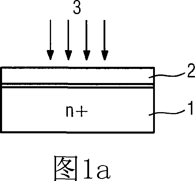
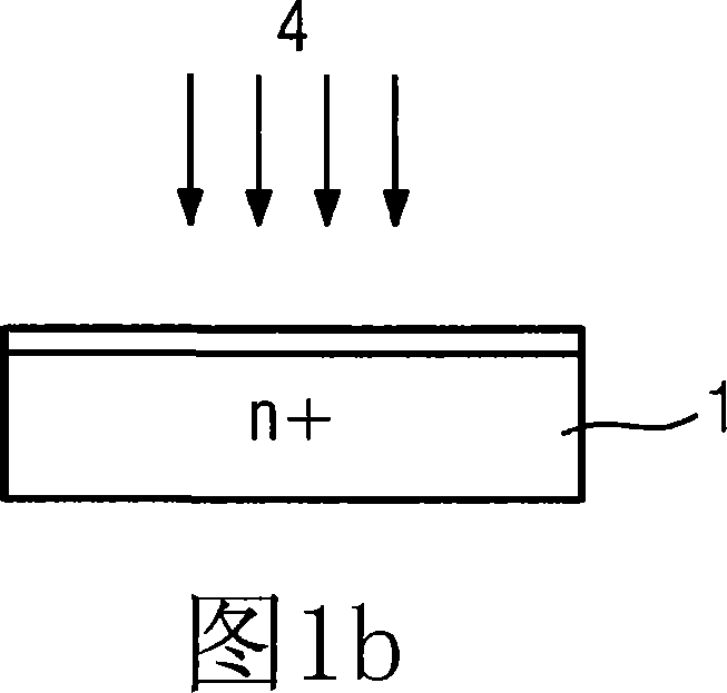
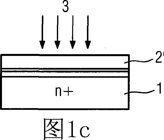
[0017] A semiconductor structure based on silicon carbide (SiC) needs to be equipped with at least one tunnel contact. The ion implantation technology used therein will be explained first with reference to FIGS. 1 a , 1 b and 2 . The use of the semiconductor structure in a SiC layer structure with corresponding electrodes, by means of which an IGBT-type component can be realized, is then explained with reference to FIGS. 3 and 4 .

[0018] FIG. 1 shows an N-type substrate 1 with a coating 2 . As shown in Figure 1a, using an energy of 25kV and a very high dose (>10 13 / cm 2 ) shallow implantation of aluminum ions3. In addition to aluminum ions, implantation of boron (B) ions may also be considered if necessary.

[0019] In an alternative as shown in Fig. 1b, a shallow implant of 25 kV is first used in substrate 1 with a very high dose (>10 13 / cm 2 ) of nitrogen ions 4, thereby forming a coating 2'. Subsequently, as shown in Figure 1a, the injection dose was very high (>...


PUM


Abstract

The invention relates to a Semiconductor structure composed from silicon carbide or kinsmanship material, which is provided with a wafer used as substrate and contact of an highness guide tunnel ahead. So use an N-type wafer, when epitaxial grow it will be adulterate reverse turn. When use a P-type doped semi-conducting material (32) to coating (P-type denotation ) a N-type adulterate wafer which used as substrate (30) for use to produce the semiconductor structure, before the P -type epitaxy immit N-type to the wafer so as to constitute the tunnel ahead contacts. Therefore, the IGBT-type component can be produced.

Description

technical field [0001] The invention relates to a wide bandgap semiconductor structure of silicon carbide or a similar material according to the preamble of claim 1 . Furthermore, the invention also relates to a corresponding method for producing such a semiconductor structure which is used in particular as a dedicated switching element. Background technique [0002] A semiconductor structure usually consists of a wafer serving as a substrate and a plurality of semiconducting layers with a defined doping arranged on top of this wafer. A semiconductor switching element can be formed on the basis of such a semiconductor structure by a corresponding configuration and with the electrodes. [0003] For a series of bipolar switches based on semiconductor materials such as silicon carbide (SiC), a P-type conductive backside made of SiC is required. Since the P-type conductive substrate (wafer) is limited by crystal growth technology, it only has a poor conductivity of several Ωcm...

Claims


Application Information

Patent Timeline
Patent Type & Authority Applications(China)
IPC IPC(8): H01L29/739H01L21/331H01L21/04
CPCH01L29/66068H01L29/7395H01L29/1608
Inventor 海因茨·米特莱纳迪特里希·斯蒂芬妮
Owner SICED ELECTRONICS DEV
Why Eureka
Try Eureka