Method for growing wide spectrum indium arsenide/aluminium gallium arsenide quantum point material

A growth method and AlGaAs technology are applied in the field of molecular beam epitaxy growth of wide-spectrum indium arsenide/AlGaAs quantum dot materials, and can solve problems such as unfavorable broadening of the emission spectrum of quantum dots.

Inactive Publication Date: 2007-09-19
INST OF SEMICONDUCTORS - CHINESE ACAD OF SCI
View PDF0 Cites 10 Cited by
  • Summary
  • Abstract
  • Description
  • Claims
  • Application Information

AI Technical Summary

Problems solved by technology

The large diffusion length makes the quantum dots tend to be uniform, which is not conducive to the broadening of the quantum dot luminescence spectrum

Method used


Image

  • Method for growing wide spectrum indium arsenide/aluminium gallium arsenide quantum point material
  • Method for growing wide spectrum indium arsenide/aluminium gallium arsenide quantum point material

Examples


Embodiment Construction

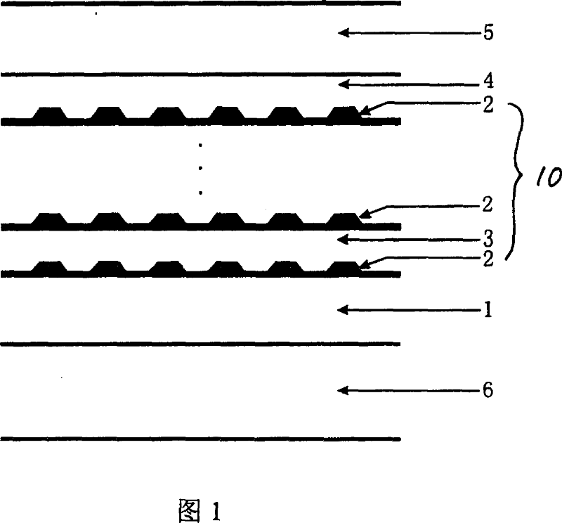
[0025] Please refer to Fig. 1. The present invention relates to a molecular beam epitaxy growth method for a wide-spectrum indium arsenide / aluminium-gallium arsenide quantum dot material. The specific implementation is as follows:

[0026] An aluminum gallium arsenide buffer layer 1 is grown. The aluminum gallium arsenide buffer layer 1 is grown on the gallium arsenide substrate 6. The aluminum gallium arsenide buffer layer 1 is a barrier layer for the following indium arsenide quantum dots 2, and has a limitation The role of carriers. The growth parameters are, specifically:

[0027] The temperature of the substrate is 600 degrees Celsius; the growth rate of AlGaAs is 0.6-1.0 μm / hour; the composition of aluminum in AlGaAs is 0.15 to 0.20; the thickness of the AlGaAs buffer layer is greater than 100 nanometers.

[0028] The aluminum gallium arsenide buffer layer 1 grown with the above parameters has high structural and optical quality, and its surface undulation is in the ran...


PUM

PropertyMeasurementUnit
thicknessaaaaaaaaaa
thicknessaaaaaaaaaa
thicknessaaaaaaaaaa

Abstract

The invention provides a growth method of wide spectrum InAs / GaAlAs quantum dot material, which is a growth method of burying self-organization quantum dot material based on molecular beam epitaxy device, wherein the method includes: choosing a substrate; preparing an GaAlAs buffer layer, as a lower barrier layer for an active region to be mentioned, on the substrate; preparing the active region, working as core part and spectrum emission region of the InAs / GaAlAs quantum dot material, on the GaAlAs buffer layer; preparing low temperature GaAlAs cover layer, as an upper barrier layer for the active region, on the active region; preparing a high temperature GaAlAs cover layer which is the outmost layer of the InAs / GaAlAs quantum dot material for protection, in this manner, the growth of material can be completed.

Description

technical field [0001] The invention relates to a molecular beam epitaxial growth method of a wide-spectrum indium arsenide / aluminum gallium arsenide quantum dot material, belonging to the technical field of semiconductor material epitaxial growth. Background technique [0002] Self-organized quantum dots show attractive application prospects in optoelectronic devices, such as lasers, detectors, and optical storage. Taking advantage of the non-uniform size distribution of self-organized quantum dots, optoelectronic devices with incoherent and wide-spectrum characteristics, such as superluminescent light-emitting tubes, can be fabricated. The luminescent wavelength of quantum dot materials is closely related to the size of quantum dots, the composition of quantum dots and the composition of barriers surrounding quantum dots. The size non-uniformity of quantum dots can be increased by optimizing the growth parameters to achieve the purpose of broadening the quantum dot lumine...

Claims


Application Information

Patent Timeline
Patent Type & Authority Applications(China)
IPC IPC(8): H01L21/20H01L33/00H01L31/18H01S5/343H01L33/06
CPCY02P70/50
Inventor 刘宁金鹏王占国
Owner INST OF SEMICONDUCTORS - CHINESE ACAD OF SCI
Why Eureka
Try Eureka