

Printed circuit boards
A technology of printed circuit boards and electromagnetic waves, which is applied in the direction of printed circuits, printed circuits, printed circuit components, etc., can solve problems such as noise interference, undesigned, or even random placement, and achieve the effect of suppressing mutual interference
- Summary
- Abstract
- Description
- Claims
- Application Information
AI Technical Summary
Problems solved by technology
Method used
Image

Examples
Embodiment Construction
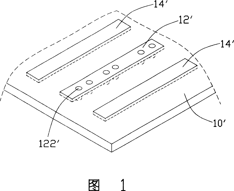
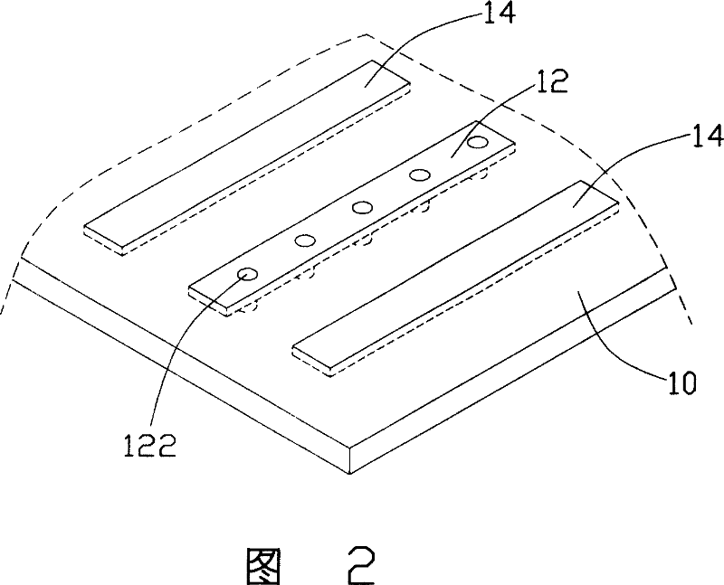
[0011] Please refer to FIG. 2 , a preferred embodiment of the printed circuit board of the present invention includes at least one signal layer 10 and a ground layer (not shown), and the signal layer 10 includes at least one isolated ground line 12 and two adjacent signal lines 14 , the isolated ground wire 12 is arranged between two adjacent signal wires 14 for reducing the interference between the signal wires 14 . Wherein, the isolated ground wire 12 is provided with a plurality of via holes 122 connected to the ground layer, and the distance between every two adjacent via holes 122 is equal, so that the resonant wavelength of the electromagnetic wave on the isolated ground wire 12 is a fixed value.
[0012] Assuming that the distance between every two adjacent via holes 122 is L, the resonant wavelength of the electromagnetic wave on the isolated ground wire 12 is λ, the resonant frequency is F0, the velocity of the electromagnetic wave in vacuum is C, and the dielectric o...
PUM
 Abstract
Description
Claims
Application Information