

Optical device
A technology of optical equipment and optical systems, applied in optics, optical components, nonlinear optics, etc., can solve problems such as defects, light transmittance reduction, peeling, etc., and achieve the effects of reducing steps, suppressing light scattering, and suppressing adhesion
- Summary
- Abstract
- Description
- Claims
- Application Information
AI Technical Summary
Problems solved by technology
Method used
Image

Examples
Embodiment 1
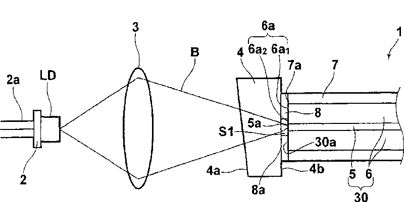
[0064] Here, a method for forming the layer 8 of the optical fiber 30 according to the above-mentioned embodiment and an example in which the formed optical fiber 30 is repeatedly attached to and detached from the dielectric block 4 will be described.
[0065] 1) The optical fiber 30 is an SI-type silica optical fiber with a core 5 diameter of 60 μm and a cladding layer 6 with a diameter of 125 μm. The incident end face 30a of the 30 is pressed against the resist so that the end face 30a is covered with the resist.
[0066] 2) Next, patterning is carried out by irradiating a laser with an oscillation wavelength of 405 nm from the end surface of the optical fiber 30 opposite to the side covered with the resist, baking at 100° C., and then developing, so that at least the incident end surface 5 a of the core 5 is resisted. etchant pattern overlay.
[0067] 3) Next, a Cr film of several μm was vacuum-deposited on the incident end face 30a of the optical fiber 30, and then the la...
Embodiment 2
[0075] Here, a method for forming the layer 8 ′ of the optical fiber 30 according to the above-mentioned embodiment and an example in which the formed optical fiber 30 is repeatedly attached to and detached from the dielectric block 4 will be described. The formation method of the layer 8' is only different in the end surface formed, which is the same as the formation method of the layer 8 in the above-mentioned embodiment 1. The emission end surface of the dielectric block 4 is patterned by a photolithography process to form a layer composed of a Cr film. layer 8'.
[0076] Then, the incident end surface 30a of the optical fiber 30 is pressed against the end surface 8b' on which the layer 8' is formed on the dielectric block 4 as described above through a connector not shown, and the attachment and detachment are repeated. From the results, it was confirmed that foreign matter adhered to the incident end face 5 a of the core 5 of the optical fiber 30 was reduced and the adhes...
PUM
 Abstract
Description
Claims
Application Information