Semiconductor memory device

A storage device and semiconductor technology, applied in information storage, static memory, digital memory information, etc., can solve the problem of difficulty in taking into account high-speed operation and low power supply voltage operation, and achieve the effect of improving the degree of freedom of design

Inactive Publication Date: 2007-10-24
PANASONIC CORP
View PDF1 Cites 5 Cited by
  • Summary
  • Abstract
  • Description
  • Claims
  • Application Information

AI Technical Summary

Problems solved by technology

[0017] As described above, it is difficult to achieve both high-speed operation and low-power-supply-voltage operation in the level shifter of conventional semiconductor memory devices.

Method used


Image

  • Semiconductor memory device
  • Semiconductor memory device
  • Semiconductor memory device

Examples


Embodiment Construction

[0051] Hereinafter, a semiconductor memory device according to an embodiment of the present invention will be described in detail with reference to the drawings.

[0052] (Embodiment 1)

[0053] A semiconductor memory device according to Embodiment 1 of the present invention will be described.

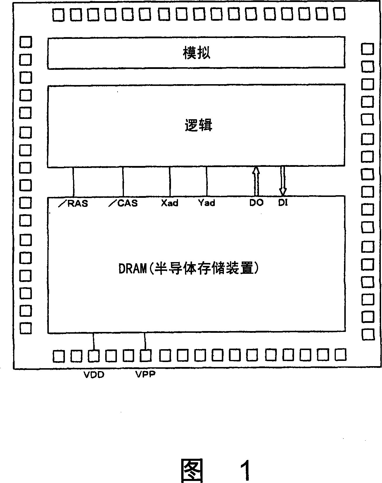
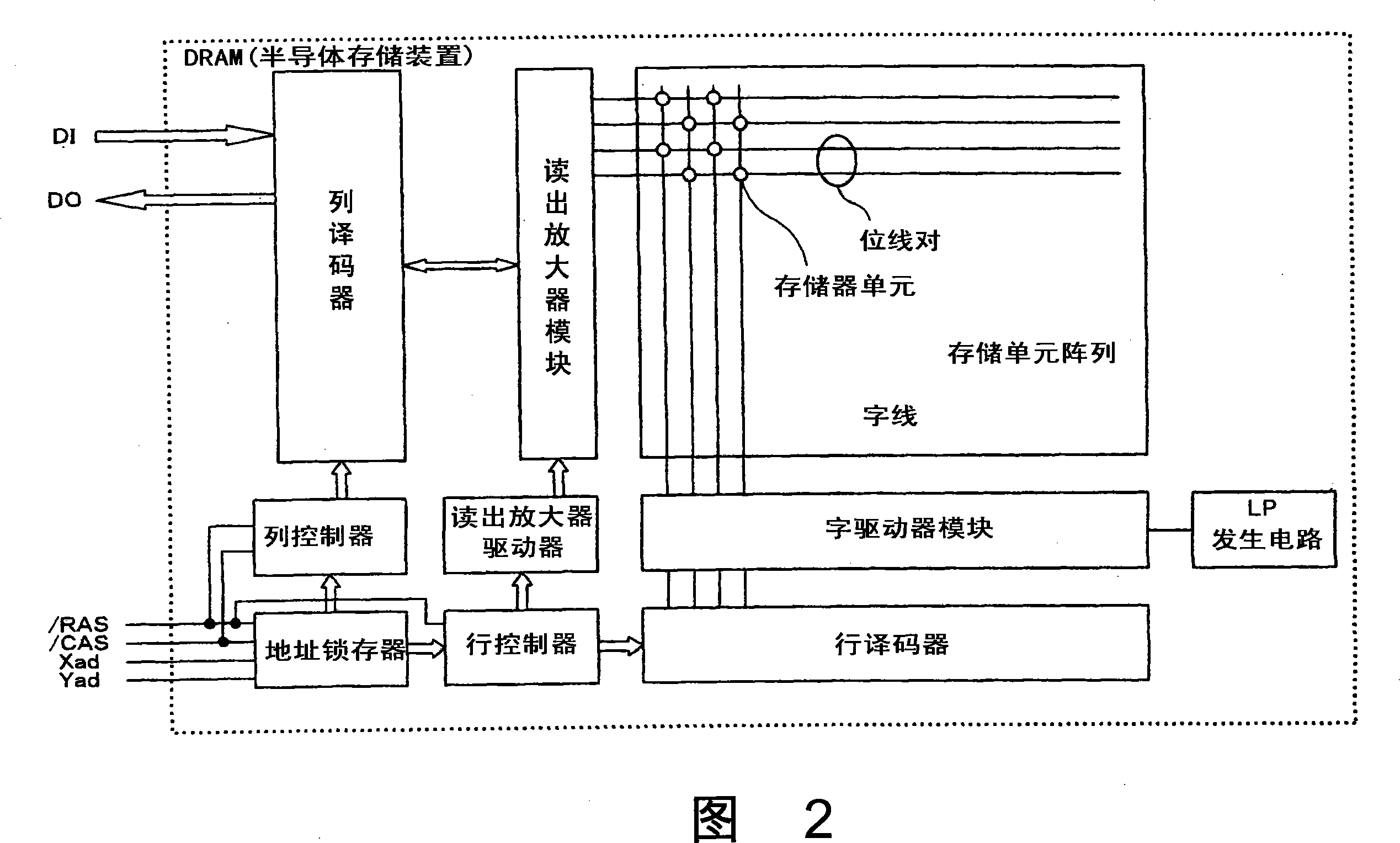
[0054] FIG. 1 is a configuration diagram of a semiconductor integrated circuit chip on which the semiconductor memory device according to the first embodiment is mounted. Here, as a semiconductor storage device, a dynamic random access memory (hereinafter, simply referred to as a DRAM) shown in FIG. 1 will be described as an example.

[0055] As shown in FIG. 1 , in a semiconductor integrated circuit, a logic circuit (logic) and an analog circuit are disposed on the same chip in addition to a DRAM. In addition, on the chip, for example, a plurality of pads are arranged on the peripheral portion, and are electrically connected to the aforementioned DRAM, logic circuit, and analog circ...


PUM


Abstract

With a semiconductor memory device according to the invention, it is possible to perform level shift of a word driver by a change in voltage at a line for a word driver P-channel control signal connected to a P-channel transistor, without a change in size of the P-channel transistor and that of an N-channel transistor, even at a low voltage of output from a row decoder. Thus, it is possible to maintain a small size ratio between the N-channel transistor and the P-channel transistor.

Description

technical field [0001] The present invention relates to a semiconductor storage device in which a memory cell array composed of a plurality of memory cells is provided, and the memory cell array is selected and driven by a word line selection circuit and a word line drive circuit to store data. Background technique [0002] Conventionally, as a semiconductor memory device, a dynamic random access memory (hereinafter, abbreviated as DRAM) in which a memory cell array composed of a plurality of memory cells is provided and data is stored in the memory cell array has been widely used. [0003] In such a DRAM, a plurality of word lines are connected to a memory cell array, and each word line of these word lines is respectively connected to a plurality of memory selection transistors constituting a word line selection circuit and a word driver constituting a word line drive circuit. driver. [0004] In the above-mentioned DRAM, if a certain word driver is selected, the word line...

Claims


Application Information

Patent Timeline
Patent Type & Authority Applications(China)
IPC IPC(8): G11C8/08G11C8/10
CPCG11C11/4082G11C8/10G11C5/147G11C11/4085G11C8/08G11C11/4087
Inventor 山田直毅折笠宪一
Owner PANASONIC CORP
Why Eureka
Try Eureka