Chip overlap structure and wafer structure for manufacturing the chip stack structure

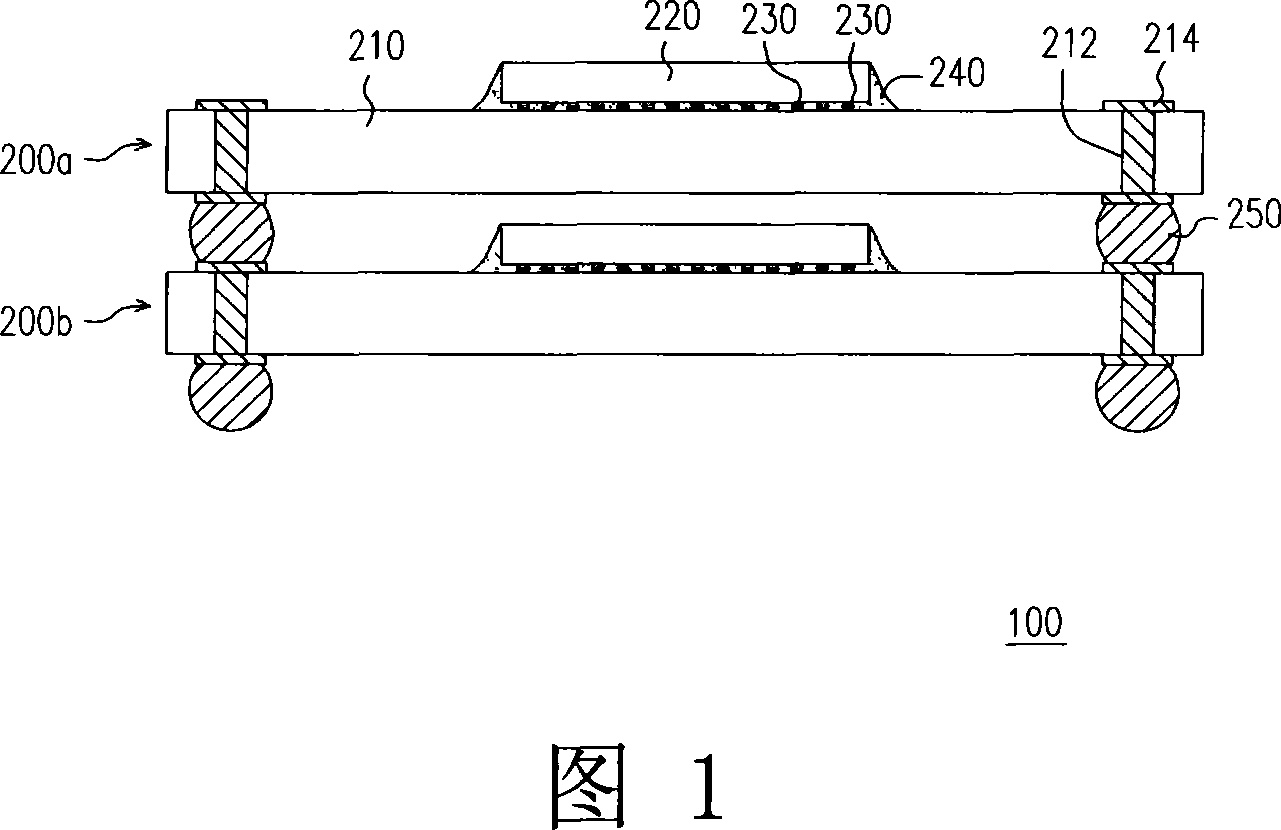
A chip stacking and chip technology, which is applied to electrical components, electrical solid-state devices, circuits, etc., can solve the problem of increasing the thickness of the chip package stack structure 100 and the difficulty of further improving and reducing the package accumulation of the chip package stack structure 100. question

Active Publication Date: 2007-10-24
ADVANCED SEMICON ENG INC
View PDF0 Cites 15 Cited by
  • Summary
  • Abstract
  • Description
  • Claims
  • Application Information

AI Technical Summary

Problems solved by technology

[0005] It is worth noting that since the package carrier 210 and the chip 220 have a certain thickness, and the bumps 230 and the solder balls 250 also have a certain height, the chip packages 200a and 200b also have a certain thickness and are difficult to reduce
Therefore, when the conventional multi-chip packages (200a, 200b...) are stacked to form the chip package stack structure 100, the thickness of the chip package stack structure 100 will often increase rapidly, thus Does not meet design needs
[0006] Therefore, under the limitation of a fixed volume or thickness, it is difficult to further improve the packing density of the chip package stack structure 100.

Method used


Image

  • Chip overlap structure and wafer structure for manufacturing the chip stack structure
  • Chip overlap structure and wafer structure for manufacturing the chip stack structure
  • Chip overlap structure and wafer structure for manufacturing the chip stack structure

Examples


Embodiment Construction

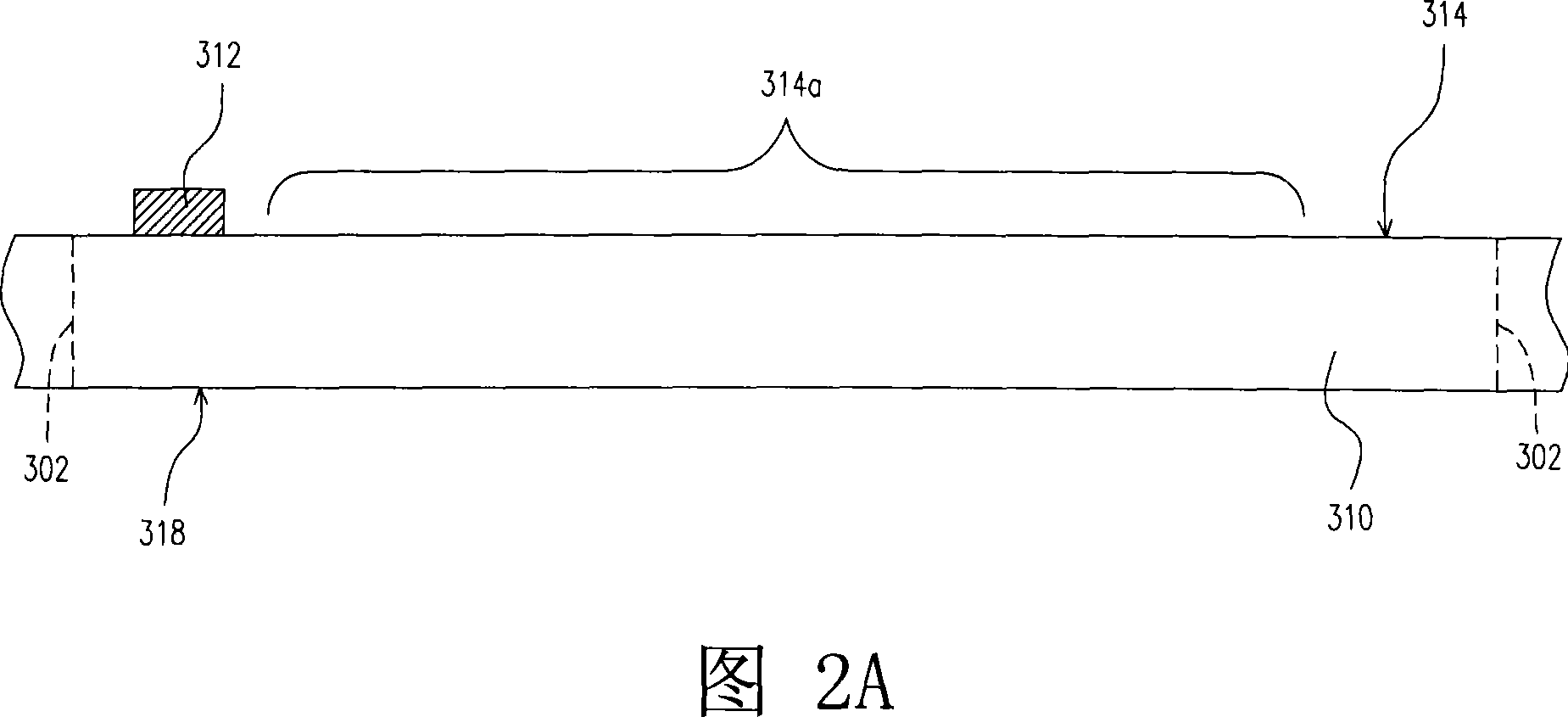
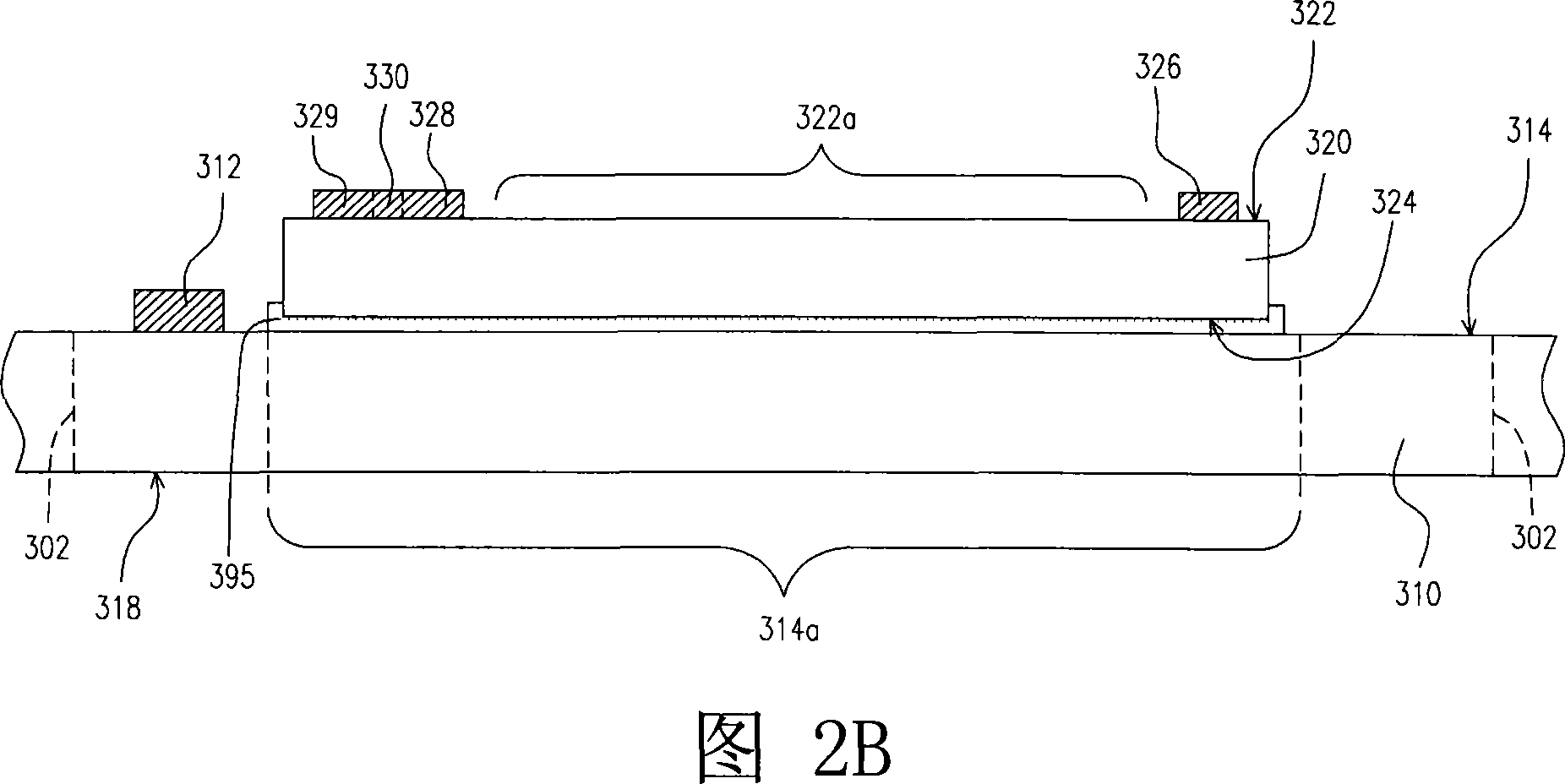
[0033] 2A-2F are schematic cross-sectional views of the fabrication process of the wafer structure according to an embodiment of the present invention. FIG. 3 is a schematic top view of FIG. 2A . Please refer to FIG. 2A and FIG. 3 together. First, a semiconductor substrate 300 is provided, which includes at least one first chip 310 . The junction 302 of two adjacent first chips 310 is marked by a straight line in FIG. 3 , and is marked by a dotted line in FIG. 2A . One or more second contacts 312 are disposed on the active surface 314 of the first chip 310, and the active surface 314 has a chip carrying area 314a, and the second contacts 312 are located outside the chip carrying area 314a.

[0034]Referring to FIG. 2B , a second chip 320 is then provided, wherein the second chip 320 has an active surface 322 and a back surface 324 . Then, the back surface 324 faces the active surface 314 of the first chip 310, and the second chip 320 is disposed in the chip carrying area 314...


PUM


Abstract

The disclosed chip stack structure comprises: two chips, a protective layer on the active face of first chip to clad the second chip, and first conductive pole inserted in the protective layer to make one end connect with first joint point and another out of the protective layer, wherein the second chip is stacked on the first one, the back face of the second chip is toward the active face of the first chip. The second chip comprises a first joint point on its active face. The product is thin.

Description

【Technical field】 [0001] The present invention relates to a chip package structure and a wafer structure for manufacturing the chip package structure, in particular to a chip stack structure (stacked structure of chips), and A wafer structure for manufacturing the chip stack structure. 【Background technique】 [0002] In today's information society, users are pursuing high-speed, high-quality, and multi-functional electronic products. As far as product appearance is concerned, the design of electronic products is moving towards the trend of light, thin, short and small. In order to achieve the above purpose, many companies incorporate the concept of systemization when designing circuits, so that a single chip can have multiple functions, so as to save the number of chips configured in electronic products. In addition, as far as electronic packaging technology is concerned, in order to meet the trend of light, thin, short and small design, packaging design concepts such as m...

Claims


Application Information

Patent Timeline
Patent Type & Authority Applications(China)
IPC IPC(8): H01L25/00H01L25/065H01L23/488H01L23/485
CPCH01L2224/12105H01L2224/32145H01L24/94H01L2224/48145H01L2224/73265H01L2224/94H01L24/73H01L2924/351
Inventor 蔡裕斌
Owner ADVANCED SEMICON ENG INC
Why Eureka
Try Eureka