Shift register circuit and image display device provided with the same

A technology of shift registers and circuits, which is applied to instruments, static indicators, etc., can solve problems such as weakening effects and difficulty in high-speed work, and achieve the effects of preventing malfunctions and speeding up and down

Inactive Publication Date: 2007-10-31
MITSUBISHI ELECTRIC CORP
View PDF1 Cites 31 Cited by
  • Summary
  • Abstract
  • Description
  • Claims
  • Application Information

AI Technical Summary

Problems solved by technology

That is, the effect achieved by the second capacitive element (C1), such as suppressing the decrease in the drive capability of the first transistor at the time of outputting the output signal, is weakened by the action of the first capacitive element (C2).
As a result, if the driving capability of the first transistor cannot be ensured sufficiently, the problem of difficulty in high-speed operation again arises.

Method used


Image

  • Shift register circuit and image display device provided with the same
  • Shift register circuit and image display device provided with the same
  • Shift register circuit and image display device provided with the same

Examples


Embodiment approach 1

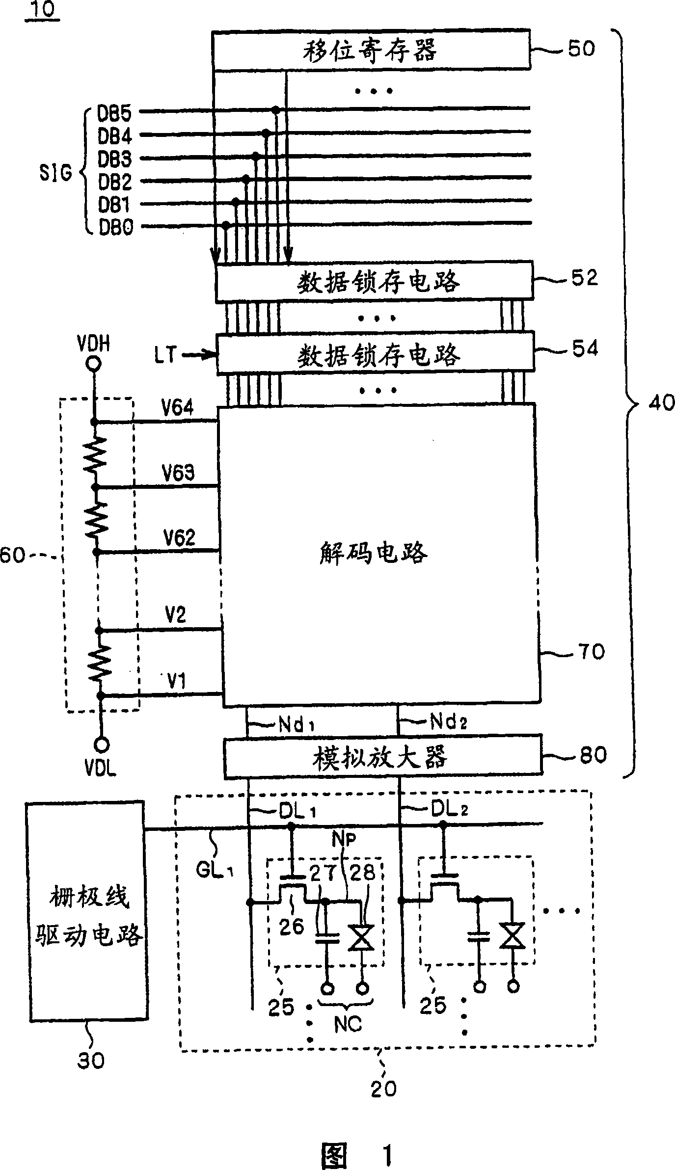
[0070] 1 is a schematic block diagram showing the configuration of a display device according to Embodiment 1 of the present invention, and shows the overall configuration of a liquid crystal display device 10 as a representative example of the display device.

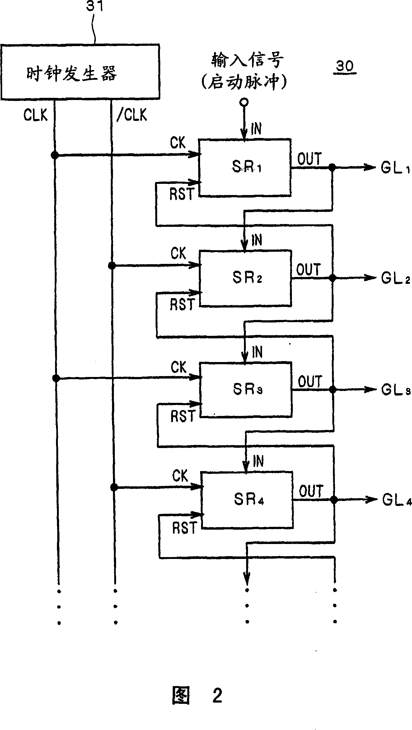
[0071] The liquid crystal display device 10 includes a liquid crystal array unit 20 , a gate line driver circuit (scanning line driver circuit) 30 , and a source driver 40 . Although it will be apparent from the description below, the shift register according to the embodiment of the present invention is mounted on the gate line driver circuit 30 .

[0072] The liquid crystal array unit 20 includes a plurality of pixels 25 arranged in a matrix. A gate line GL is respectively arranged for each row of pixels (hereinafter also referred to as a "pixel line") 1 、GL 2 ...... (collectively referred to as "gate lines GL"), in addition, data lines DL1, DL2... (collectively referred to as as "data line DL"). In FIG. 1, the p...

Embodiment approach 2

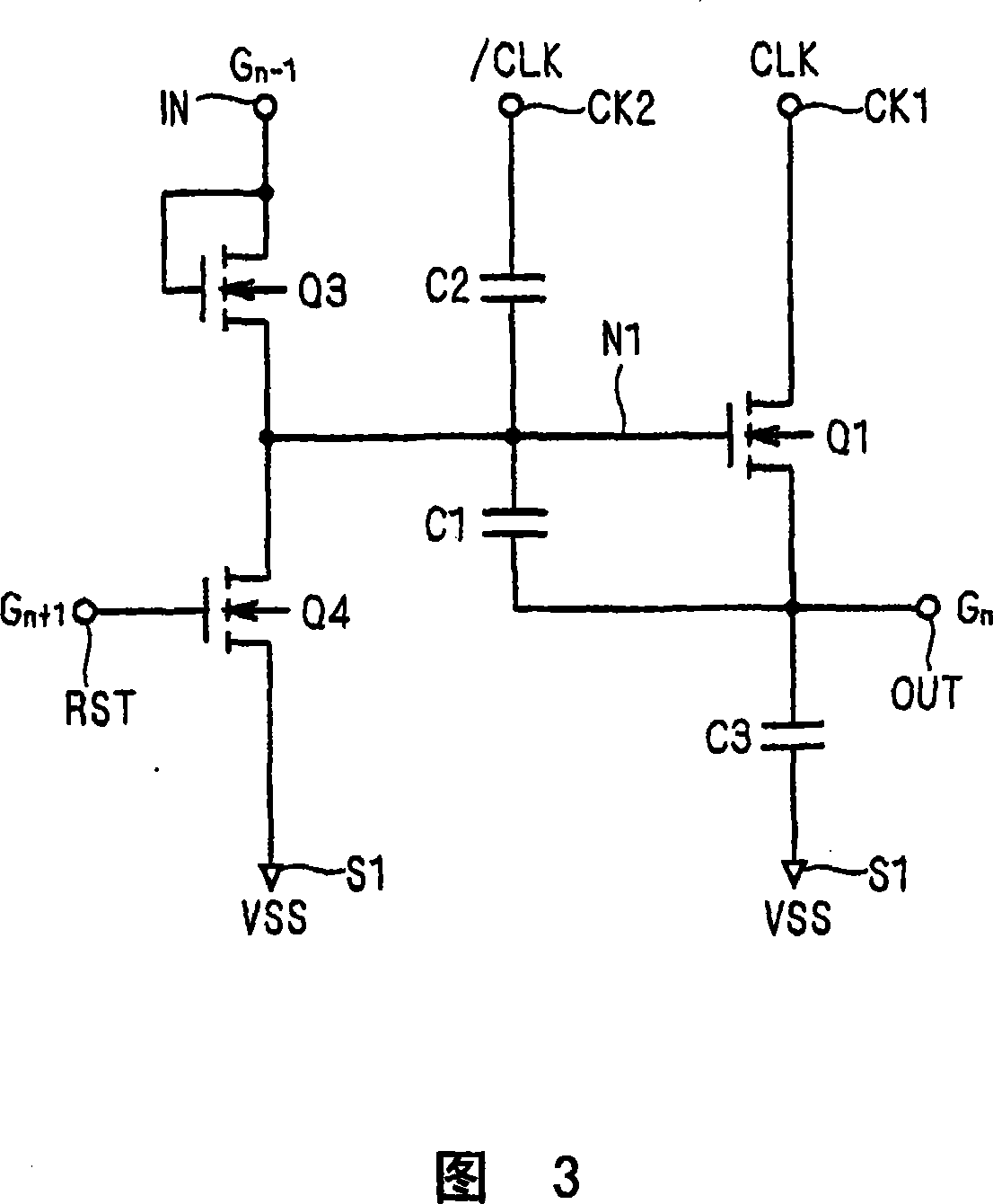
[0146] In the unit shift register SR of Embodiment 1 n (Figure 7), using the output signal G of the previous stage n-1 to perform charging of node N1. In other words, the unit shift register SR n The output signal G n Not only for the gate line GL n is charged and is also used to charge the lower-level unit shift register SR n+1 The node N1 is charged.

[0147] Capacitive components accompanying the node N1 of the unit shift register SR include the capacitance of the capacitive element C1 and the gate capacitance of the transistor Q1. In Embodiment 1, this capacitive component becomes a part of the load capacitance C3 of the output terminal OUT of each unit shift register SR, and becomes a factor of slowing down of the rising speed of the output signal. This hinders the speed-up of the operation of the unit shift register SR, which becomes a problem.

[0148] In Embodiment 2, the unit shift register SR which can solve this problem is proposed. FIG. 12 is a circuit diag...

Embodiment approach 3

[0154] A display device in which a shift register of a gate line driver circuit is formed of amorphous silicon TFT (a-Si TFT) is easy to increase in size and has high productivity, and is widely used, for example, in a notebook PC screen or a large-screen display device.

[0155] On the contrary, it can be seen that the a-Si TFT has a problem that if the gate electrode continues to be positively biased, the threshold voltage will shift to the positive direction, and its drive capability will decrease. For example, in the circuit of Embodiment 1 (FIG. 7), since the clock signal / CLK is repeatedly input to the gate of the transistor Q2, the threshold voltage of the transistor Q2 shifts, and the driving capability thereof gradually decreases, and there is a concern that the output terminal OUT cannot be discharged. . At this time, in the non-selected state, the charge that should not be discharged from the node N1 through the transistor Q5 is accumulated in the output terminal OU...


PUM


Abstract

In a shift register circuit, a defective operation while an output signal is not outputted and a drive capability lowering while the output signal is outputted are prevented. A unit shift register comprises a first transistor for supplying a clock signal inputted to a first clock terminal to an output terminal, and the first transistor is driven by a drive circuit. A second transistor is connected between the gate of the first transistor and the output terminal and has a gate connected to the first clock terminal. The second transistor connects the gate of the first transistor to the output terminal based on the clock signal when the gate of the first transistor is at L (Low) level.

Description

technical field [0001] The present invention relates to a shift register circuit, in particular to a shift register circuit composed only of field effect transistors of the same conductivity type, which is used in, for example, a scanning line driving circuit of an image display device. Background technique [0002] In an image display device such as a liquid crystal display device (hereinafter referred to as a "display device"), gate lines (scanning lines) are provided for a plurality of pixel rows (pixel lines) of a display panel in which a plurality of pixels are arranged in a matrix. During one horizontal period of the display signal, the gate lines are sequentially selected and driven to update the displayed image. As a gate line driver circuit (scanning line driver circuit) for sequentially selecting and driving pixel lines, that is, gate lines, a shift register that performs shift operation once in one frame period of a display signal can be us...

Claims


Application Information

Patent Timeline
Patent Type & Authority Applications(China)
IPC IPC(8): G09G3/20G09G3/36
Inventor 飞田洋一
Owner MITSUBISHI ELECTRIC CORP
Why Eureka
Try Eureka