Integrated circuit with memory cells comprising a programmable resistor and method for addressing memory cells comprising a programmable resistor

A technology for memory cells and integrated circuits, which is applied in the field of integrated circuits containing memory cells including programmable resistors and for addressing memory cells including programmable resistors, can solve problems such as inability to provide sufficient power

Active Publication Date: 2007-11-07
NXP BV
View PDF5 Cites 2 Cited by
  • Summary
  • Abstract
  • Description
  • Claims
  • Application Information

AI Technical Summary

Problems solved by technology

[0010] However using normal sized (N)MOS transistors does not provide enough power per transistor size which would be applied

Method used


Image

  • Integrated circuit with memory cells comprising a programmable resistor and method for addressing memory cells comprising a programmable resistor
  • Integrated circuit with memory cells comprising a programmable resistor and method for addressing memory cells comprising a programmable resistor
  • Integrated circuit with memory cells comprising a programmable resistor and method for addressing memory cells comprising a programmable resistor

Examples


Embodiment Construction

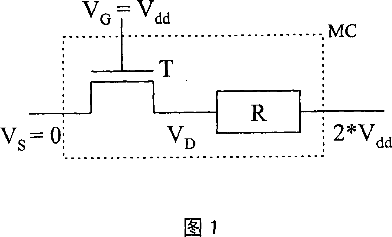
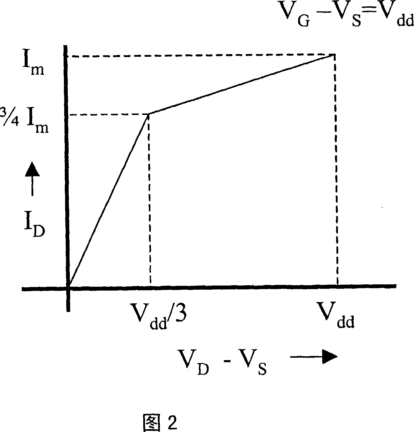
[0032] FIG. 1 shows a circuit diagram of a basic phase change memory cell according to a first embodiment of the present invention. If the selected value of the programmable resistor R is such that V d -V s about V dd / 3, then the best power dissipation of the programmable resistor can be obtained in the memory cell.

[0033] therefore,

[0034] P opt m *V dd

[0035] P opt =3 / 4*I m *2 / 3*V dd =_*I m *V dd

[0036] R opt =(2 / 3V dd ) / (3 / 4*I m )=8 / 9*(V dd / I m )

[0037] P opt ≤ I m *V dd

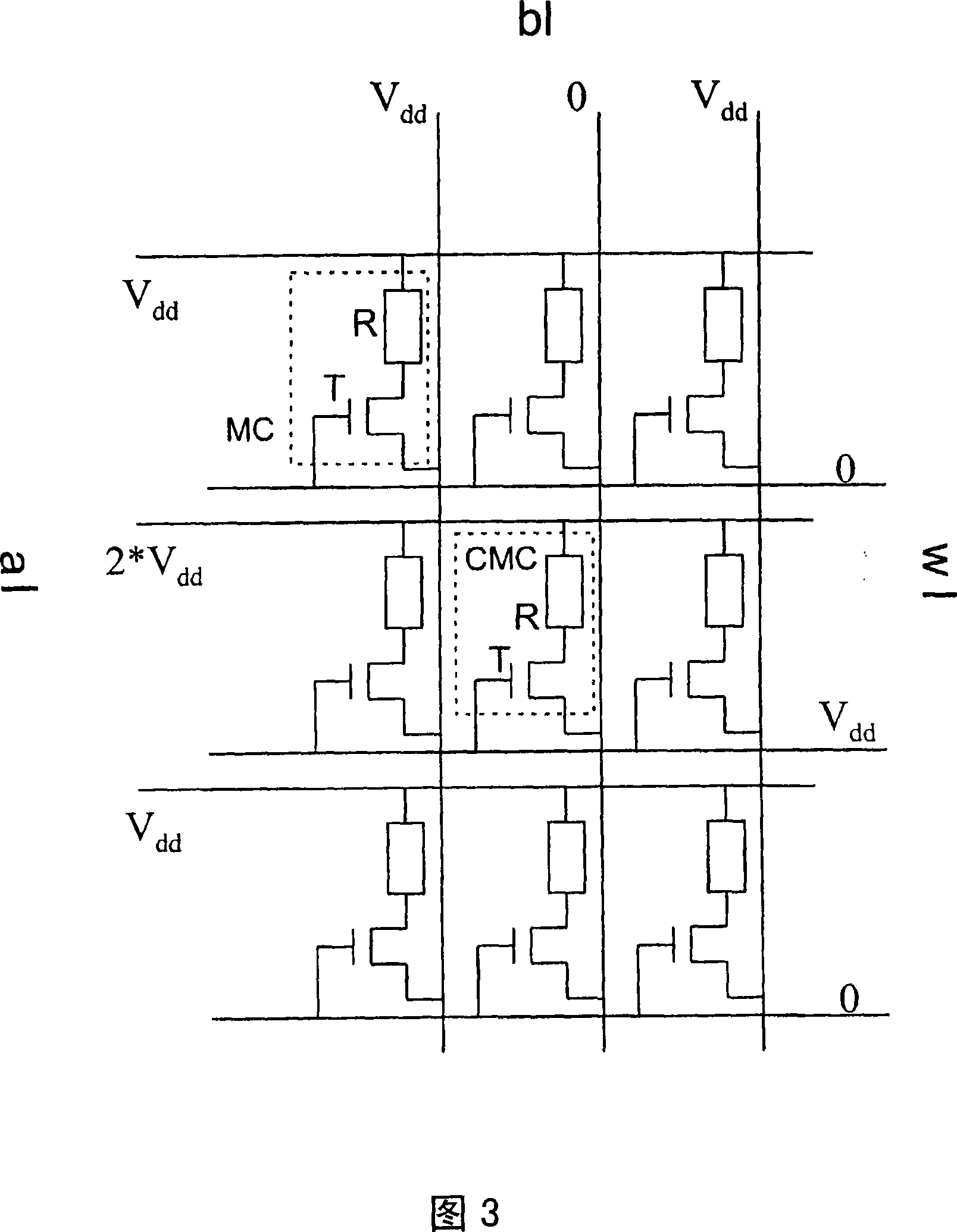
[0038] One side of the programmable phase change resistor R is connected to the drain terminal of the NMOS transistor T, 2*V dd The voltage is applied to the other side of the programmable phase change resistor R. When the source terminal is connected to the common ground V s =0, the voltage V dd Applied to the drain terminal of the NMOS transistor T.

[0039] The value of resistor R must be designed so that the following equation holds:

[0040] V D =2*V dd -I D ...


PUM


Abstract

A module comprises a bus invert encoder (24) for determining whether a set of data bits should be inverted prior to transmission over a communication bus. The bus invert encoder (24) produces a bus invert signal BI which controls a selective inversion means (28), for example a multiplexer. A partial fault detection encoder (32) determines one or more temporary check bits from the set of data bits, substantially in parallel with the bus invert encoder (24). Thus, the one or more temporary check bits are determined based on the assumption that the set of data bits are to be transmitted without inversion from the selective inversion means (28). A logic unit (34) is provided for correcting the one or more temporary check bits, if necessary, based on the bus invert signal produced by the bus invert encoder (24). The module has the e advantage of enabling the temporary check bits to be determined in parallel with the bus invert encoding, thereby reducing latency, with the logic unit being used to correct the check bits, if necessary, prior to transmission over the communication bus.

Description

technical field [0001] The invention relates to an integrated circuit containing a memory cell comprising a programmable resistor and a method for accessing a memory cell comprising a programmable resistor. Background technique [0002] A new type of semiconductor storage device based on the use of so-called phase-change materials as data storage means, that is, phase-change memory, could become the next generation of non-volatile memory. These phase change memories explore reversible changes in the crystal structure of chalcogenide alloys. [0003] Typically, a phase change memory comprises an array of constituent cells, where each cell contains a phase change material for storing data. By incorporating chalcogenide alloys into integrated circuits, such cells can be used as fast-switching programmable resistors. Specifically, this phase change memory cell includes a series arrangement of a resistor made of phase change material and some kind of selection device. Phase ch...

Claims


Application Information

Patent Timeline
IPC IPC(8): G11C16/02
CPCG11C2213/79G11C2013/0054G11C2013/0071G11C13/0004
Inventor 马特吉·H·R·兰赫斯特弗朗西斯库斯·P·威德斯霍芬
Owner NXP BV
Why Eureka
Try Eureka