Fin-shaped field-effect transistor with concrete contact window and making method

A field effect transistor and manufacturing method technology, applied in the field of fin field effect transistor and its manufacturing, can solve the problems of uncontrollable voltage, product and method without suitable structure and manufacturing method, inconvenience and the like

Active Publication Date: 2007-06-13
TAIWAN SEMICON MFG CO LTD
View PDF0 Cites 0 Cited by
  • Summary
  • Abstract
  • Description
  • Claims
  • Application Information

AI Technical Summary

Problems solved by technology

However, the structural design of the above-mentioned fin-shaped channel also makes it a silicon on insulator (SOI) structure, and becomes a floating body (floating body), and its voltage cannot be controlled.
[0008] It can be seen that the above-mentioned existing fin field effect transistor and its manufacturing method obviously still have inconvenience and defects in structure, manufacturing method and use, and need to be further improved urgently.
In order to solve the problems existing in fin field effect transistors and their manufacturing methods, relevant manufacturers have tried their best to find a solution, but for a long time no suitable design has been developed, and there is no suitable general product and method. The structure and manufacturing method can solve the above problems, which is obviously a problem that the relevant industry is eager to solve

Method used


Image

  • Fin-shaped field-effect transistor with concrete contact window and making method
  • Fin-shaped field-effect transistor with concrete contact window and making method
  • Fin-shaped field-effect transistor with concrete contact window and making method

Examples


Embodiment Construction

[0048] In order to further explain the technical means and effects that the present invention takes to achieve the intended purpose of the invention, the specific implementation methods, Structure, characteristic and effect thereof are as follows in detail.

[0049] According to the above, the present invention provides a fin field effect transistor with a body contact window and a manufacturing method thereof, so as to control the voltage of the fin channel and to measure the thickness and quality of the gate oxide layer.

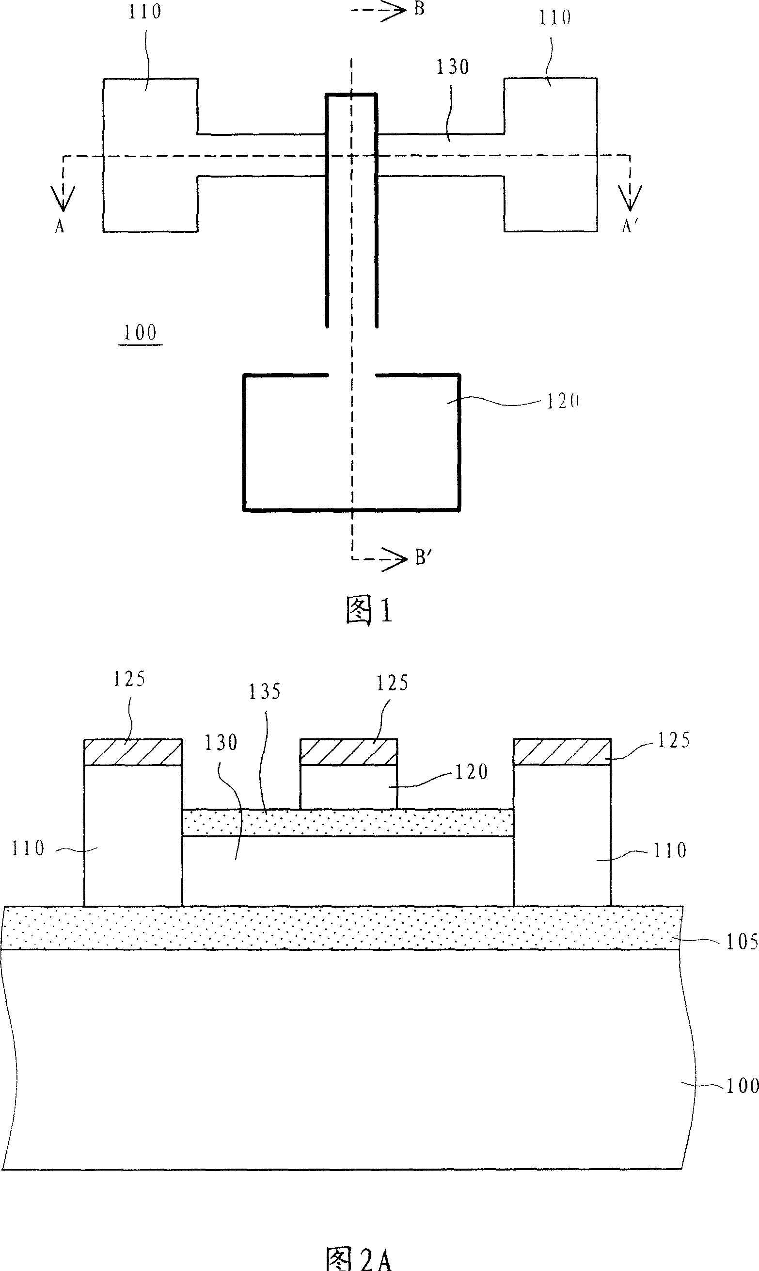
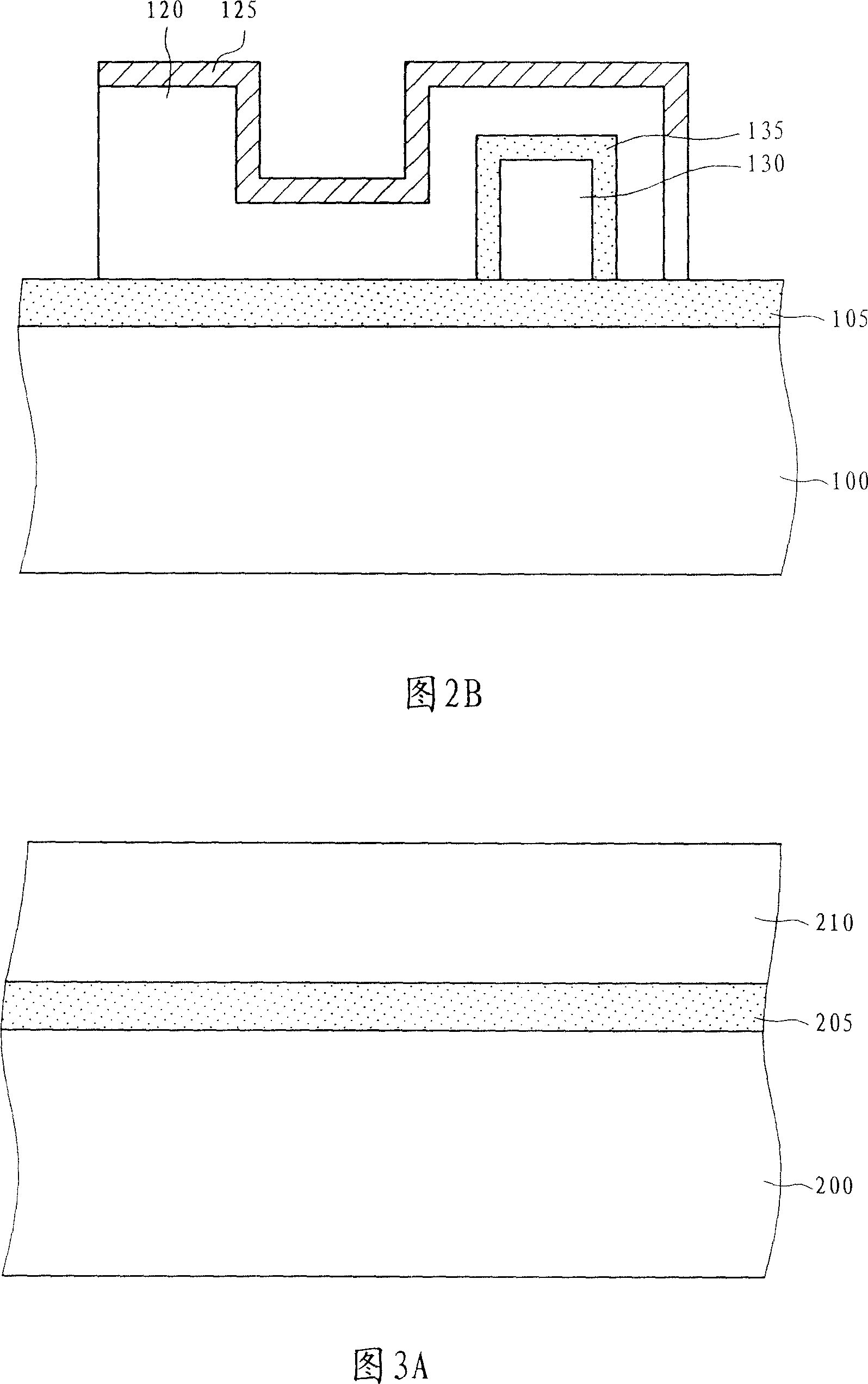
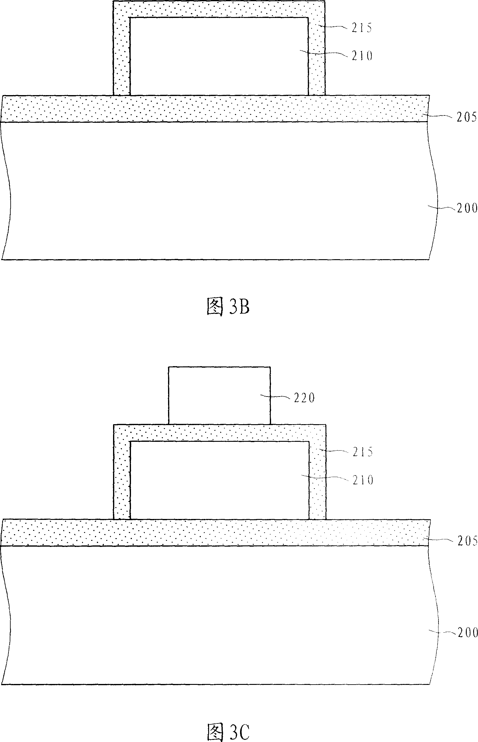
[0050] Please refer to FIGS. 3A-3D , which are cross-sectional views illustrating a manufacturing process of a fin field effect transistor with a body contact window according to a preferred embodiment of the present invention. In FIG. 3A , a first insulating layer 205 and a semiconductor layer 210 are sequentially formed on a substrate 200 . The material of the first insulating layer 205 can be, for example, silicon oxide, and its formation method can be...


PUM


Abstract

The field-effect transistor (TET) includes fin type channel, source electrode, drain electrode, solid contact window, gate dielectric layer (DL), and gate electrode. Source and drain electrodes are connected to two ends of the fin type channel. Being positioned at one side of fin channel, solid contact window through wire connect the channel. Gate dielectric layer covers surface of fin channel. Being positioned at the other side of fin channel, gate electrode crosses over the channel. Method for preparing TET includes steps: forming insulating layer and semiconductor layer, patterning semiconductor layer to form T channel; at same time, forming source and drain electrodes, and solid contact window at three end points of T channel; forming gate DL, and forming conducting layer; patterning the conducting layer in order to form gate electrode crossing over lateral channel of the T channel; gate electrode and solid contact window are located at two sides of lateral channel.

Description

technical field [0001] The present invention relates to a semiconductor device, and in particular to a fin field effect transistor with a body contact window and a manufacturing method thereof. Background technique [0002] Since the development of integrated circuits in the 1960s, their component density has increased dramatically. While the component density of integrated circuits is increasing, the size of the components is also continuously shrinking. In particular, the thickness of the gate electrode and the length of the channel between the source and drain electrodes have required dimensions ranging from micrometers to nanometers. In the process of shrinking the size of components, the operating characteristics, reliability, and durability of components, as well as the reliability and cost of component manufacturing, have always been important issues. [0003] In the process of component miniaturization, several problems have also arisen, including short channel eff...

Claims


Application Information

Patent Timeline
IPC IPC(8): H01L29/78H01L21/336
Inventor 杨国男詹宜陵陈豪育杨富量胡正明
Owner TAIWAN SEMICON MFG CO LTD
Why Eureka
Try Eureka