Probing apparatus and probing method
A technology for inspection devices and conveying devices, which is applied in transportation and packaging, single semiconductor device testing, semiconductor/solid-state device testing/measurement, etc. It can solve the problems of insufficient space, enlarged floor space, and inability to continue to expand the floor space, etc. , to achieve the effect of improving inspection efficiency and saving space
- Summary
- Abstract
- Description
- Claims
- Application Information
AI Technical Summary
Problems solved by technology
Method used
Image

Examples
no. 1 approach
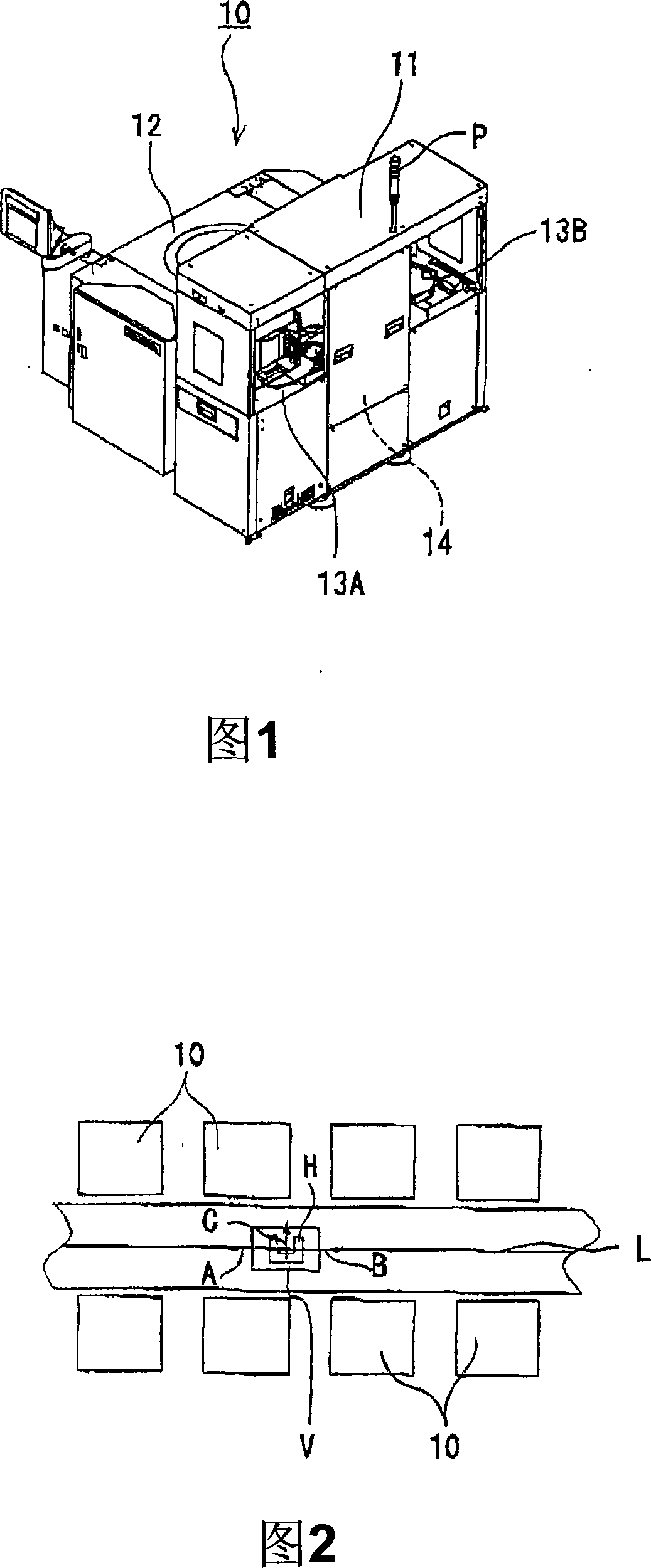
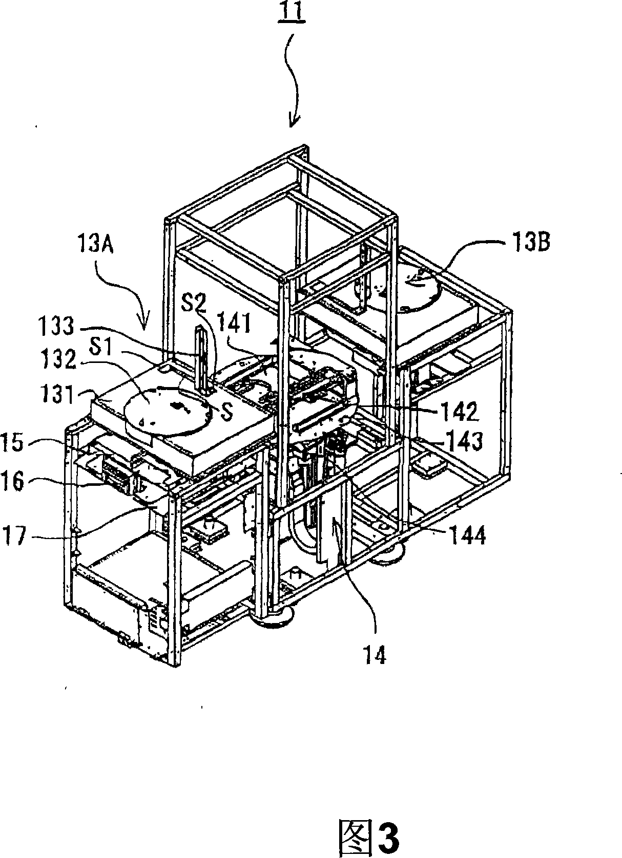
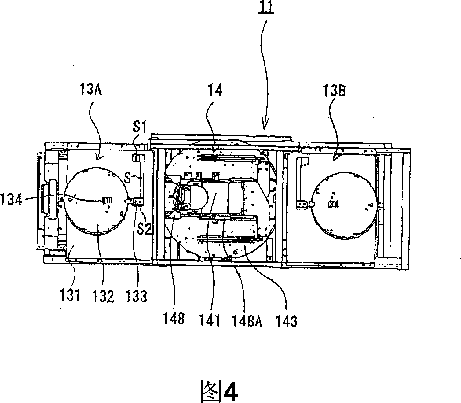
[0063] The inspection apparatus 10 of this embodiment includes, for example, as shown in FIG. side of chamber 12. The load chamber 11 includes two first and second load ports 13A and 13B at the front and back, on which a wafer cassette (cassette) (not shown) accommodating a plurality of wafers is placed, and the first and second load ports 13A and 13B are arranged. The wafer transfer device (see FIG. 3 ) 14 between 13B is driven under the control of a control device (not shown). For example, as shown in FIG. 2 , a plurality of inspection devices 10 are arranged on both sides of a transfer line L formed in a clean room. In this embodiment, the conventional loading chamber having one loading port at the front is changed to the loading chamber 11 having the front and rear first and second loading ports 13A, 13B, and the footprint is substantially the same as that of the existing inspection device. , the function of the loading chamber 11 can be expanded without enlarging the fl...
no. 2 approach
[0096] In the inspection apparatus 10A of this embodiment, for example, as shown in FIGS. 9 and 10 , the first loading port 13A has a structure in which a FOUP is placed as a wafer cassette C, and a switch 21 for automatically opening and closing the lid of the FOUP is provided, and a buffer The table 15 is configured substantially in the same manner as the inspection device 10 of the first embodiment except that the structure is different. Therefore, the same or equivalent parts as those of the first embodiment will be described with the same reference numerals, and the FOUP will be described as the wafer cassette C.
[0097] The first load port 13A in this embodiment has a direction changing mechanism as shown in FIGS. 9 and 10 . This direction changing mechanism includes: a turntable 132 provided on the opening of the base 131 so as to form the same plane as the upper surface of the base 131 having an opening thereon; The loading unit 135 of the cartridge C. The turntable...
no. 3 approach
[0107] The inspection device 10B of this embodiment, for example, as shown in FIG. Except for accommodating the wafer cassette C, it has substantially the same configuration as the inspection device 10 of the first embodiment. Therefore, the same or equivalent parts as those of the first embodiment will be described with the same reference numerals.
[0108] That is, as shown in FIG. 12 , the third loadport 13C is disposed below the first loadport 13A, and has substantially the same structure as the first and second loadports 13A and 13B. The transfer arm 141 of the wafer transfer device 14 is raised and lowered by the first and second elevating drive mechanisms (not shown), facing the first load port 13A or the third load port 13C, and carries wafers in and out of each cassette C. When loading and unloading wafers in the wafer cassette C of the first load port 13A, as shown by the solid line in FIG. The second lifting drive mechanism moves up and down between the upper and ...
PUM
 Abstract
Description
Claims
Application Information