Optimized wire bonding of an integrated modulator and laser diode on a mount
A technology for optical semiconductor components and mounting substrates, which is applied in semiconductor devices, semiconductor lasers, semiconductor/solid-state device components, etc., and can solve problems such as difficulty in obtaining output waveform quality
- Summary
- Abstract
- Description
- Claims
- Application Information
AI Technical Summary
Problems solved by technology
Method used
Image
Examples
Embodiment 1
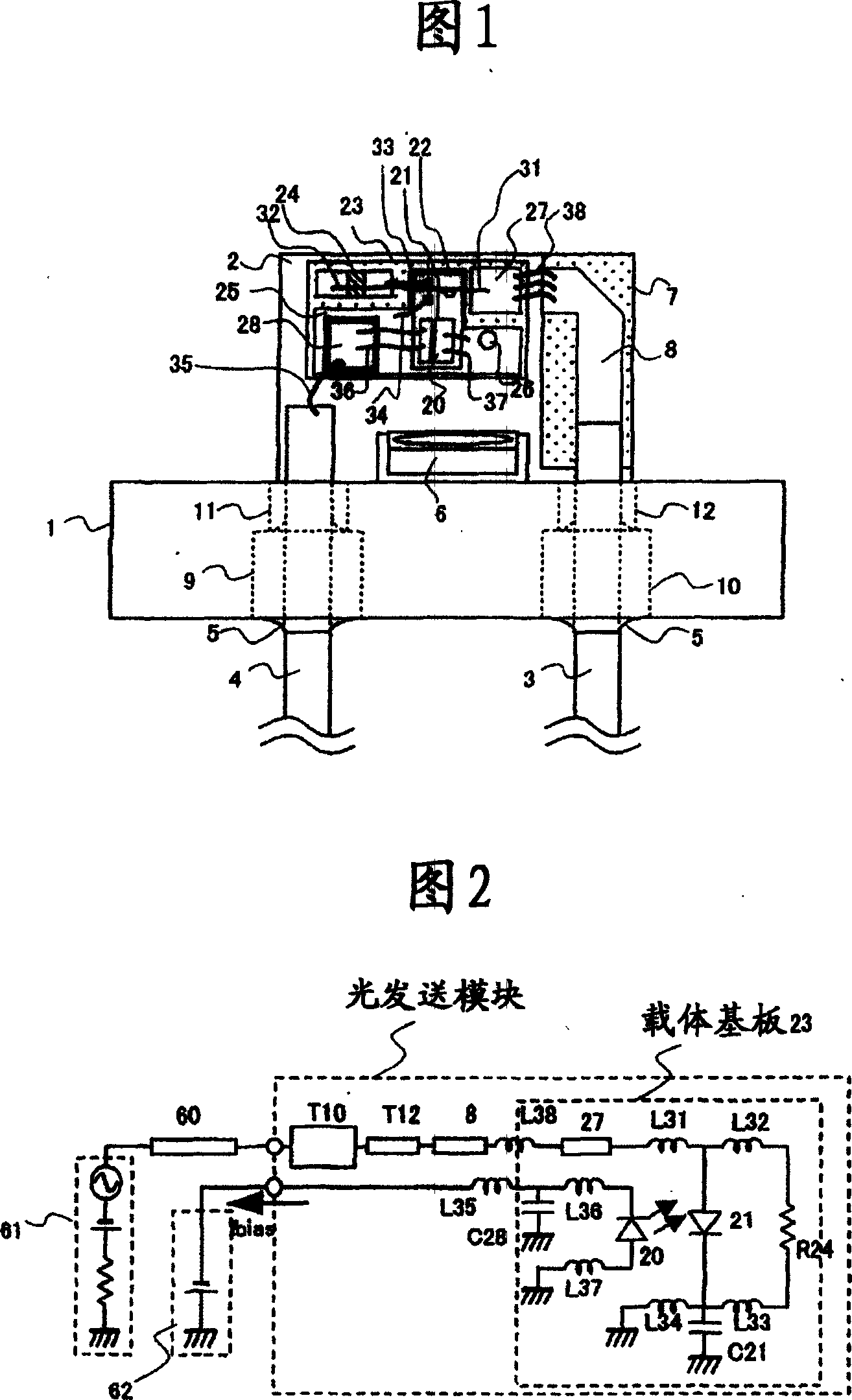
[0041] A first embodiment of the present invention will be described with reference to FIGS. 1 to 3 and FIGS. 9 to 13 .
[0042] 1 is a structural diagram showing the main parts of the optical transmission module in this embodiment, FIG. 2 is a main circuit diagram showing the optical transmission module, FIG. Figure 10 is a diagram showing the optical output waveform of the optical transmission module, and Figures 11 to 13 respectively show the keys connected to the optical modulator element Graphs of excess gain, 3dB band, and input reflection characteristic S11 when the inductance of the bond wire changes.
[0043] First, the configuration of the optical transmission module will be described using FIG. 1 . The optical transmission module uses a CAN type (a structure in which terminals are drawn from one side of a cylinder) package frame, 1 is the metal rod, and 2 is a metal base for mounting the main part. Cylindrical lead pins 3 and 4 are provided through cylindrical thr...
Embodiment 2
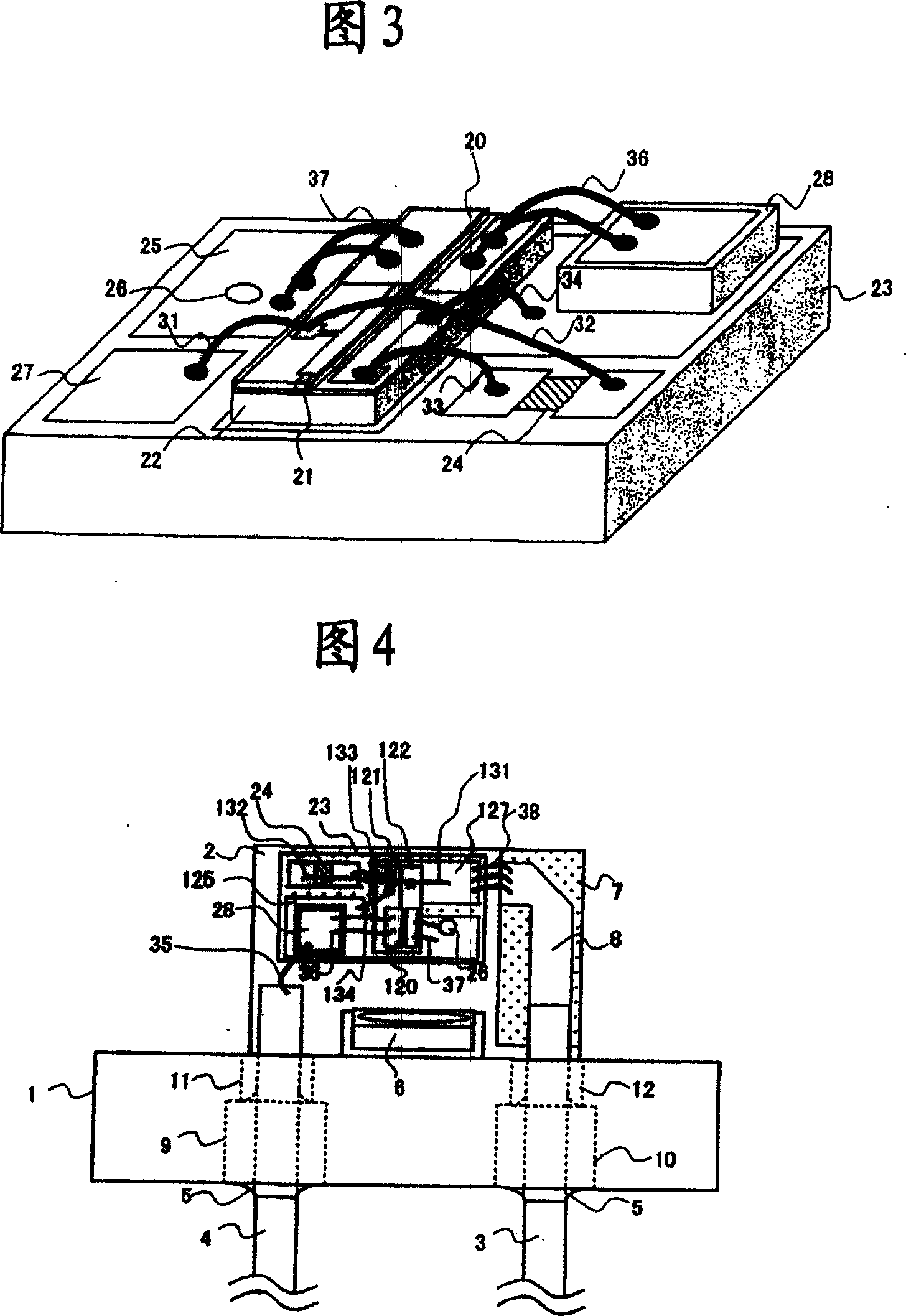
[0081] A second embodiment of the present invention will be described with reference to FIGS. 4 to 6 and FIGS. 19 to 22.
[0082] Fig. 4 is a structural diagram showing the main parts of the optical transmission module in this embodiment, Fig. 5 is a main circuit diagram showing the optical transmission module, Fig. 6 is a detailed view of the carrier substrate part, and Fig. 19 shows the input reflection of the present embodiment As a graph of the characteristic S11, FIG. 20 is a graph showing the small-signal pass characteristic S21.
[0083] As shown in FIG. 4 and FIG. 6 , the main difference from Embodiment 1 is that the arrangement of the anode and cathode of the surface electrodes of the semiconductor chip 122 is reversed left and right and the input transmission line 127 is extended to the light modulator element 121. lower part. Separate rear electrodes are provided on the rear of the semiconductor chip 122 at the respective lower parts of the light modulator element ...
Embodiment 3
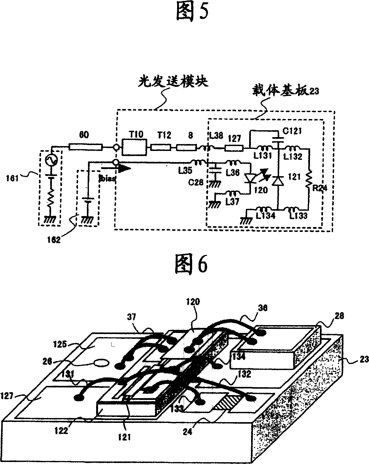
[0091] A third embodiment of the present invention will be described with reference to FIGS. 7 and 8 .
[0092] FIG. 7 is a configuration diagram showing a main part of the optical transmission module in this embodiment, and FIG. 8 is a main circuit diagram showing the optical transmission module. The main difference from the second embodiment described above is that the optical modulator element 21 is driven by a differential electrical modulation signal.
[0093] First, the configuration of the optical transmission module will be described using FIG. 7 . The optical transmission module uses a CAN-type package frame, 1 is its metal rod, and 2 is a metal pedestal for mounting the main part. Columnar lead pins 3 , 4 are provided through cylindrical through holes 209 , 210 in the metal rod 1 , and are fixed by a sealing glass 5 . The relay substrates 205 and 207 and the carrier substrate 223 are mounted on the metal base 2 . The transmission line 206 is provided on the relay ...
PUM
| Property | Measurement | Unit |
|---|---|---|
| impedance | aaaaa | aaaaa |
| impedance | aaaaa | aaaaa |
| impedance | aaaaa | aaaaa |
Abstract
Description
Claims
Application Information


