Semiconductor element and its manufacturing method

A manufacturing method and semiconductor technology, applied in the direction of semiconductor/solid-state device manufacturing, semiconductor devices, electrical components, etc., can solve problems such as limited stress in the channel region, and achieve the goals of increasing stress, low power consumption, and suppressing short-channel effects Effect

Inactive Publication Date: 2007-11-14
UNITED MICROELECTRONICS CORP
View PDF0 Cites 5 Cited by
  • Summary
  • Abstract
  • Description
  • Claims
  • Application Information

AI Technical Summary

Problems solved by technology

[0006] Although the above-mentioned local mechanical stress control method is simple to operate, it is limited to improve the stress of the channel region at present.

Method used


Image

  • Semiconductor element and its manufacturing method
  • Semiconductor element and its manufacturing method
  • Semiconductor element and its manufacturing method

Examples


Embodiment Construction

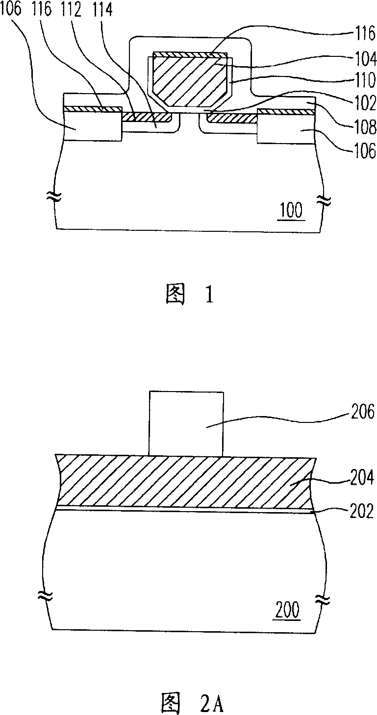
[0047] FIG. 1 is a cross-sectional view of a semiconductor device according to an embodiment of the invention. First, please refer to FIG. 1, the semiconductor element is, for example, an NMOS transistor, including a semiconductor substrate 100, a gate dielectric layer 102, a gate 104, a source / drain region 106, a stress layer 108, a An oxide layer 110 , a lightly doped region 112 , a ring implant region 114 and a metal silicide 116 are lined.

[0048] Wherein, the semiconductor substrate 100 is, for example, a silicon substrate or a substrate with silicon on an insulating layer, and the gate dielectric layer 102 is disposed on the semiconductor substrate 100, and its material is, for example, silicon oxide.

[0049] The gate 104 is disposed on the gate dielectric layer 102, and its material is, for example, doped polysilicon, and the top area of ​​the gate 104 is larger than the bottom area. In this way, since the contact area between the gate 104 and the gate dielectric lay...


PUM


Abstract

The invention is a semiconductor component, comprising a substrate, a gate dielectric layer, a gate, a source/drain region, and a stress layer, where the gate dielectric layer is arranged on the substrate, the gate is arranged on the gate dielectric layer and the area of the top of the gate is more than that of the bottom; in addition, the source/drain region is arranged in the substrate on two sides of the gate, and the stress layer is arranged on the substrate and covers the gate and the source/drain region.

Description

technical field [0001] The present invention relates to a semiconductor element and a manufacturing method thereof, in particular to a semiconductor element and a manufacturing method thereof which can improve operating performance through local mechanical stress control. Background technique [0002] In semiconductor elements, high-speed operation and low power consumption are often achieved by reducing the size of the element. However, with the continuous improvement of component integration, the current miniaturization of component size is approaching the limit. It is necessary to develop other methods of reducing component size to achieve the purpose of high-speed operation and low power consumption. [0003] Therefore, in the prior art, a method of controlling the stress of the channel region of the semiconductor transistor is proposed to solve the problem that the miniaturization of the element size is approaching the limit. This method uses stress to change the latti...

Claims


Application Information

Patent Timeline
Patent Type & Authority Applications(China)
IPC IPC(8): H01L29/78H01L29/423H01L21/336H01L21/28
Inventor 张惠贞林建廷许哲华陈亮玮李孟麟萧维沧
Owner UNITED MICROELECTRONICS CORP
Why Eureka
Try Eureka