Manufacturing method of superthin liquid crystal box
A manufacturing method and liquid crystal cell technology, applied in the direction of instruments, nonlinear optics, optics, etc., can solve the problems of low yield rate and high process requirements, and achieve the effects of saving production costs, low process requirements, and cheap prices
- Summary
- Abstract
- Description
- Claims
- Application Information
AI Technical Summary
Problems solved by technology
Method used
Image

Examples
Embodiment 1
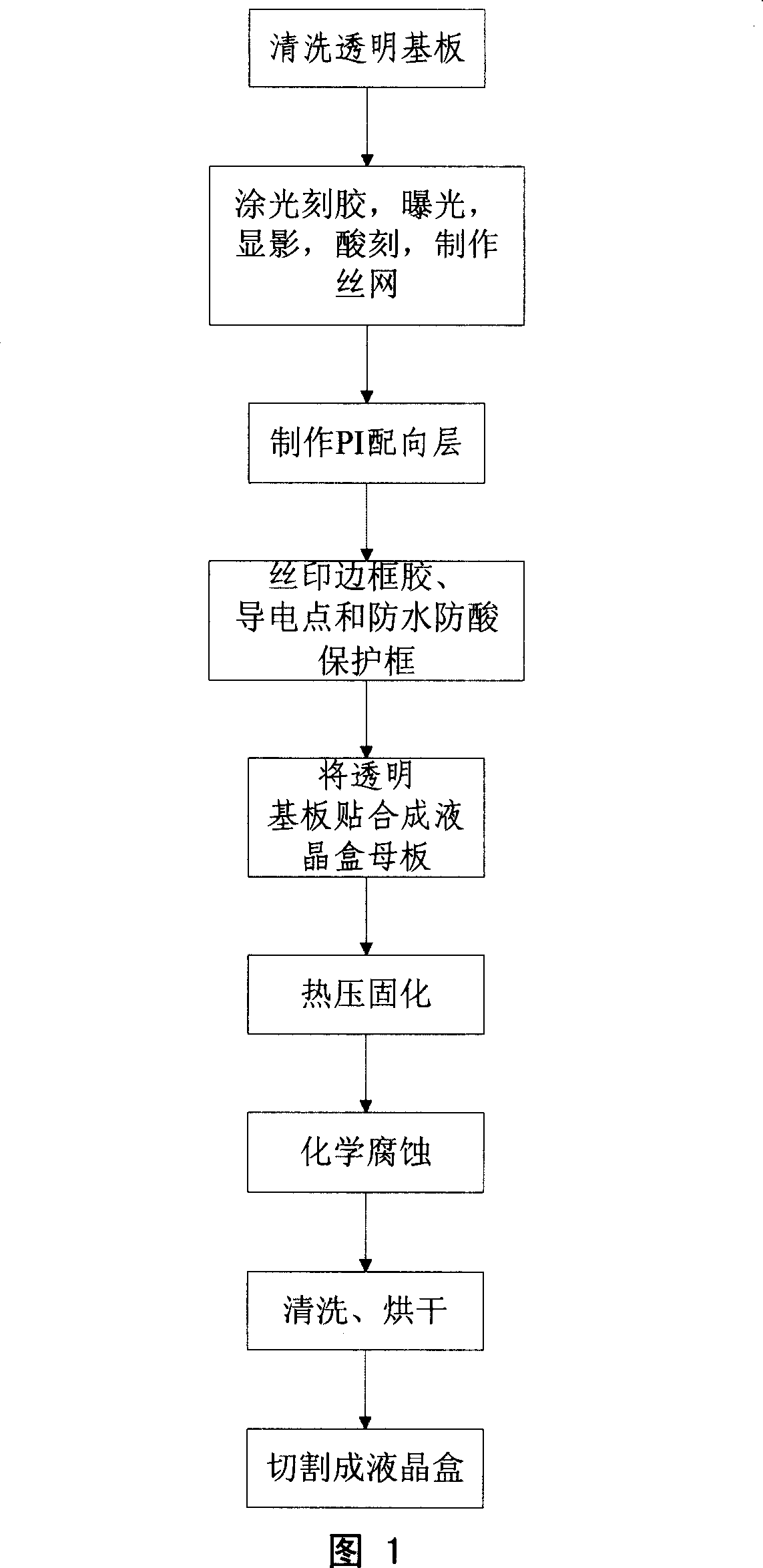
[0040] Embodiment 1, as shown in Figure 1, the manufacturing method of ultra-thin liquid crystal cell comprises the following steps:
[0041] The first step is to clean the upper and lower transparent substrates 1 and 2 successively with acetone, ultrasonic waves, alcohol, pure water, brush, etc., to remove various harmful impurities or oil stains adsorbed on the surface of the transparent substrates, and to prevent contamination of the PI alignment layer and liquid crystal raw materials .
[0042] In the second step, apply photoresist on the transparent substrate, perform exposure after pre-curing, develop, and perform acid etching after curing (using the protective effect of photoresist, etching with a mixture of hydrochloric acid, nitric acid and pure water), engraving Produce required patterns such as dot matrix graphics and leads;
[0043] In addition, the exposure technology is used to produce the silk screen required to make the waterproof and acid-proof protective fra...
Embodiment 2
[0054] Embodiment 2, the difference from Embodiment 1 is that in step 7, the thickness after etching is set to 0.6mm, the thickness of the liquid crystal cell motherboard before chemical etching is 1.03mm, and the concentration percentage of chemical etchant is hydrofluoric acid 20%, 2% hydrochloric acid, 10% nitric acid, 0.5% surfactant, and pure water for the rest. The etching temperature is 22+ / -2 degrees. After 40 minutes of chemical etching, the thickness of the liquid crystal cell motherboard is reduced to 0.59mm. The etching results are shown in Table 1. The flatness (peak-trough) before etching is 0.080-0.075mm, and the flatness (peak-trough) after etching is 0.051-0.045mm. Therefore, after chemical etching, the high flatness of the transparent substrate is not affected. The degree can reach the technical requirement of + / -30um.
[0055] Compared with the existing ultra-thin liquid crystal manufacturing method, the method has the characteristics of low process requirem...
PUM
| Property | Measurement | Unit |
|---|---|---|
| Thickness | aaaaa | aaaaa |
| Thickness | aaaaa | aaaaa |
Abstract
Description
Claims
Application Information
 - R&D
- Intellectual Property
- Life Sciences
- Materials
- Tech Scout
- Unparalleled Data Quality
- Higher Quality Content
- 60% Fewer Hallucinations
Browse by: Latest US Patents, China's latest patents, Technical Efficacy Thesaurus, Application Domain, Technology Topic, Popular Technical Reports.
© 2025 PatSnap. All rights reserved.Legal|Privacy policy|Modern Slavery Act Transparency Statement|Sitemap|About US| Contact US: help@patsnap.com