Composite semiconductor device and method of manufacturing the same

一种复合器件、半导体的技术,应用在半导体/固态器件制造、半导体器件、电固体器件等方向,能够解决混色的特性变差等问题,达到可靠性优异、质量稳定性优异的效果

Inactive Publication Date: 2007-12-19
STANLEY ELECTRIC CO LTD
View PDF4 Cites 0 Cited by
  • Summary
  • Abstract
  • Description
  • Claims
  • Application Information

AI Technical Summary

Problems solved by technology

Thus, the interval between adjacent devices is extended, so that the characteristic of color mixing deteriorates

Method used


Image

  • Composite semiconductor device and method of manufacturing the same
  • Composite semiconductor device and method of manufacturing the same
  • Composite semiconductor device and method of manufacturing the same

Examples


Embodiment 1

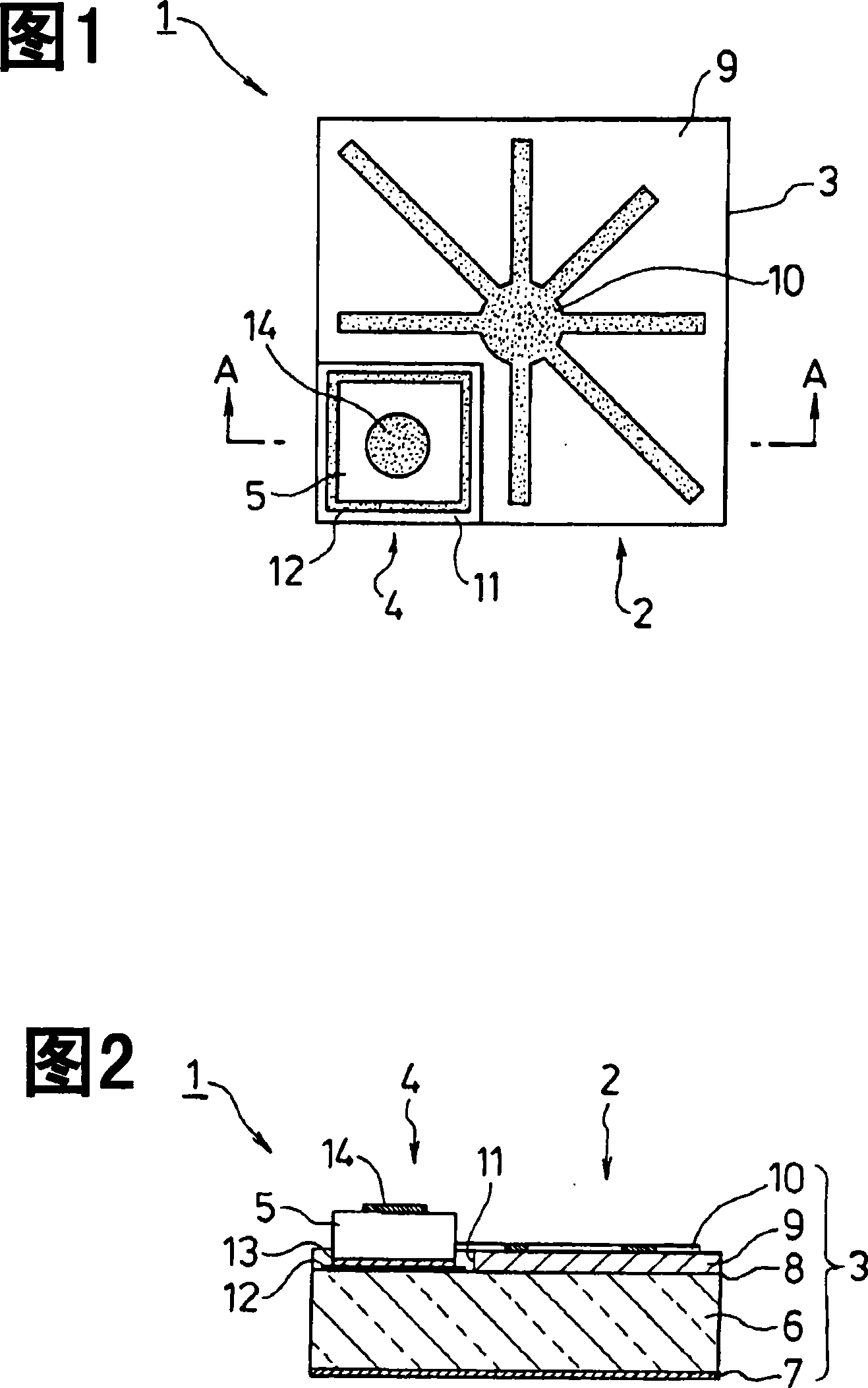
[0045] 1 is a plan view of Embodiment 1 of a semiconductor composite device according to the present invention, and FIG. 2 is a cross-sectional view along A.A of FIG. 1 .

[0046] A semiconductor composite device (semiconductor composite device, hereinafter referred to simply as "composite device") 1 includes a first semiconductor light emitting device (hereinafter referred to simply as "first light emitting device") 3 for constituting a first light emitting region 2; and a second semiconductor A light emitting device (hereinafter referred to as “second light emitting device”) 5 for constituting the second light emitting region 4 .

[0047] The first light emitting device 3 is configured as follows. The material is suitably selected from Si, Al having desired properties such as high electrical conductivity, high transmittance, high thermal conductivity and high strength 2 o 3 , SiC and GaP to form a common substrate 6 . First external connection electrodes 7 are formed on o...

Embodiment 2

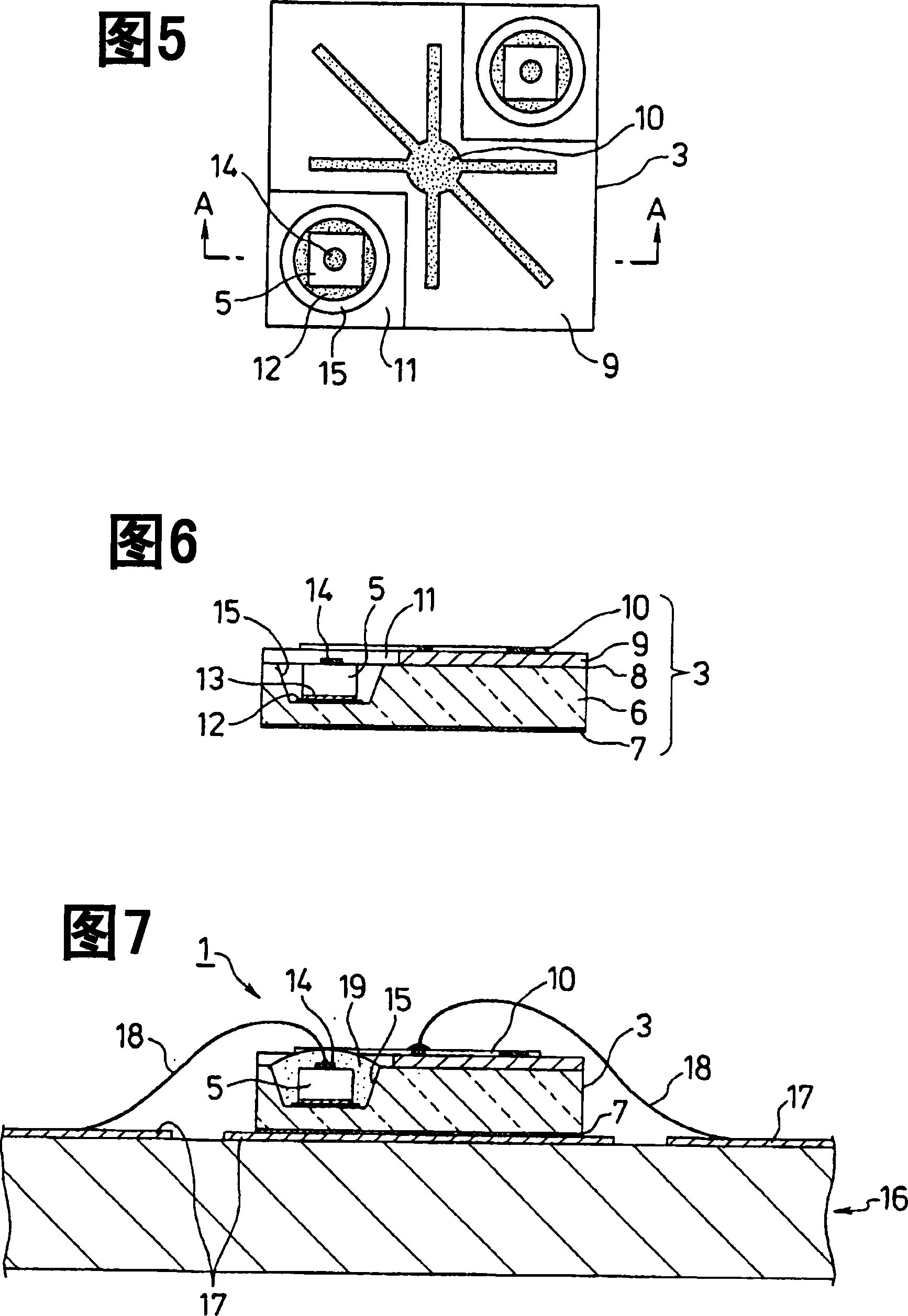
[0054] 5 is a plan view of Embodiment 2 of the semiconductor composite device according to the present invention, FIG. 6 is a cross-sectional view along A-A of FIG. 5, and FIG. 7 is an installation view.

[0055] In the present invention, corresponding grooves 11 are formed in the first light emitting device 3 at two opposite positions of the common substrate 6 where the second external connection electrode 10 and the growth layer 9 do not exist. A recess 15 is formed in the common substrate 6 in such a manner as to be exposed through the bottom of each groove 11 .

[0056] The second light emitting device bonding electrode 12 is formed on the inner bottom of the recess 15 . The eutectic junction between the lower electrode 13 on the second light emitting device 5 and the bonding electrode 12 fixes the second light emitting device 5 in the recess 15 and also enables electrical conduction between the two electrodes.

[0057] Other structures are similar to the above-mentioned ...

Embodiment 3

[0064] 8 is a sectional view of Embodiment 3 of the semiconductor composite device according to the present invention, and FIGS. 9 and 10 are mounting views.

[0065] In this embodiment 3, different from embodiment 2, the second external connection electrode 10 on the first light emitting device 3 and the upper side electrode 14 on the second light emitting device 5 have corresponding upper side surfaces on the same plane. In order to secure the positional relationship between the electrodes 10 and 14 , the first light emitting device 3 is manufactured to have a thickness greater than that of the second light emitting device 5 . In addition, the depth of the recess 15 formed in the common substrate 6 is determined in consideration of the thickness of the second light emitting device 5 .

[0066] A bumpball 28a composed of Au or the like is formed on the second external connection electrode 10, and a bump ball 28b also composed of Au or the like is formed on the second light em...


PUM


Abstract

The disclosed subject matter provides a composite semiconductor device which can include a common substrate, a first semiconductor light emitting structure, and a second semiconductor light emitting structure. The first semiconductor light emitting structure can include an epitaxial grown layer containing a light emitting layer formed on part of the common substrate either directly or via a bonding layer. The second semiconductor light emitting structure can be provided in a notch at at least one location to which the epitaxial grown layer is not bonded, or in a recess formed in the notch at one location. The disclosed subject matter also provides a method of manufacturing a composite semiconductor device having the above-described and other structures.

Description

technical field [0001] The present invention relates to a semiconductor composite device and a manufacturing method thereof. More particularly, the present invention relates to a semiconductor composite device including a plurality of light emitting units on the same substrate and a method of manufacturing the same. Background technique [0002] A semiconductor light emitting source has been proposed which includes a plurality of light emitting units having correspondingly different emission spectra formed on the same substrate made of semiconductor material or on the same device (listed below). [0003] They include: (1) semiconductor composite light-emitting devices, which include a semiconductor crystal layer having a plurality of active layers (light-emitting layers) sequentially grown on the same substrate, wherein the active layers have correspondingly different emission spectra (For example, see Japanese Patent Laid-Open Document 1: No. 3298390); (2) LED display, whi...

Claims


Application Information

Patent Timeline
Patent Type & Authority Applications(China)
IPC IPC(8): H01L25/00H01L25/075H01L21/50H01L33/00H01L33/02H01L33/50H01L33/62
CPCH01L2224/16225H01L2224/48465H01L33/60H01L2924/0002H01L2224/48091H01L33/20H01L2224/73265H01L25/0756H01L2224/8592H01L2224/05573H01L2224/05568H01L2924/00014H01L2224/32145H01L2924/00H01L2224/05599
Inventor 多田康广半谷明彦
Owner STANLEY ELECTRIC CO LTD
Why Eureka
Try Eureka