Method for producing directionally solidified silicon ingots

A technology for directional solidification and polycrystalline silicon ingots, which can be used in self-solidification methods, chemical instruments and methods, self-area melting methods, etc., and can solve problems such as reducing production costs.

Active Publication Date: 2007-12-19
REC SOLAR NORWAY AS
View PDF1 Cites 4 Cited by
  • Summary
  • Abstract
  • Description
  • Claims
  • Application Information

AI Technical Summary

Problems solved by technology

To date no one has succeeded in significantly reducing production costs while producing from conventional silicon feedstock qualities the expected silicon feedstock purity required for PV solar cell performance

Method used


Image

  • Method for producing directionally solidified silicon ingots

Examples


Embodiment 1

[0012] Embodiment 1 (prior art)

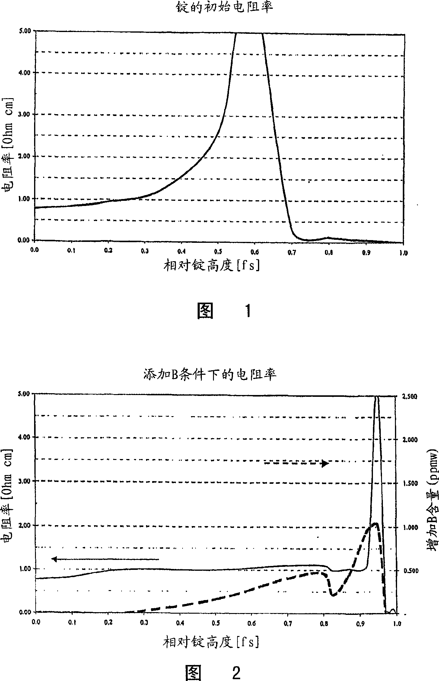
[0013] Directional solidified silicon ingots were produced from a silicon feedstock initially containing 0.8 ppma boron and 3.6 ppma phosphorous. The transition from p-type material to n-type material in a silicon ingot occurs at approximately 60% of the height of the solidified ingot. The resistivity of the as-prepared silicon ingot is shown in Figure 1, from which it can be seen that the transition from p-type material to n-type material occurs at about 60% of the ingot height.

Embodiment 2

[0014] Embodiment 2 (the present invention)

[0015] The same silicon raw material in Example 1 was used to prepare directionally solidified silicon ingots. Boron is continuously added to the remaining molten silicon when approximately 50% of the ingot has solidified. As can be seen in Figure 2, the transition from p-type material to n-type material occurs at greater than 90% of the height of the solidified ingot. The amount of boron added to the silicon melt is also shown in FIG. 2 .

[0016] By comparing the results of Example 1 and Example 2, it can be seen that the transition from p-type material to n-type material moves from about 60% of the ingot height to greater than 90% of the silicon crystal height.

[0017] Thus, with the present invention, it is possible to significantly increase the fraction of directionally solidified ingots (solidified as p-type material or n-type material).


PUM


Abstract

The present invention relates to a method for the production of directionally solidified Czochralski, float zone or multicrystalline silicon ingots or thin sheets or ribbon for making wafers for solar cells from silicon feedstock initially containing between 0.2 ppma and 10 ppma boron and between 0.1 ppma and 10 ppma phosphorous. If the boron content in the silicon feedstock is higher than the phosphorous content, the boron content in the molten silicon is kept higher than the phosphorous content during the directional solidification process by adding boron to the molten silicon in order to extend the part of the directionally solidified ingot or the thin sheet or ribbon solidifying as p-type material. If the content of phosphorous in the silicon feedstock is higher than the boron content, the phosphorous content in the molten silicon is kept higher than the boron content during the directional solidification process by adding phosphorous to the molten silicon in order to extend the part of the ingot or the thin sheet or ribbon solidifying as n-type material.

Description

technical field [0001] The present invention relates to a method for the preparation of directionally solidified Czochralski, floating zone or polycrystalline silicon ingots, thin wafers or strips for the production of photovoltaic (PV) solar cells. Background technique [0002] In recent years, ultrapure virgin electronic-grade polysilicon (EG-Si) produced from suitable shavings, chips, and rejects in the electronic chip industry has been used in the fabrication of photovoltaic solar cells. The recent downturn in the electronics industry has resulted in idle polysilicon capacity being used to produce lower-cost grades suitable for producing PV solar cells. This has temporarily eased the tight market demand for solar-grade polysilicon (SoG-Si) supply quality. As demand for electronic equipment returns to normal levels, it is expected that a major share of polysilicon capacity will return to the supply of the electronics industry, leaving the PV industry undersupplied. The ...

Claims


Application Information

Patent Timeline
IPC IPC(8): C30B15/04H01L31/0288C30B29/06C30B11/04C30B13/10H01LH01L31/18
CPCH01L31/182C30B11/04C30B29/06Y02E10/546C30B15/04C30B13/10Y02P70/50
Inventor C·德思洛夫K·弗里斯塔德
Owner REC SOLAR NORWAY AS
Why Eureka
Try Eureka