

Layout method and semiconductor device
A layout method and semiconductor technology, applied in special data processing applications, instruments, computer-aided design, etc., can solve problems such as increasing the cost of semiconductor devices, and achieve the effects of improving attributes, small area, and reducing costs
- Summary
- Abstract
- Description
- Claims
- Application Information
AI Technical Summary
Problems solved by technology
Method used
Image

Examples
no. 1 example
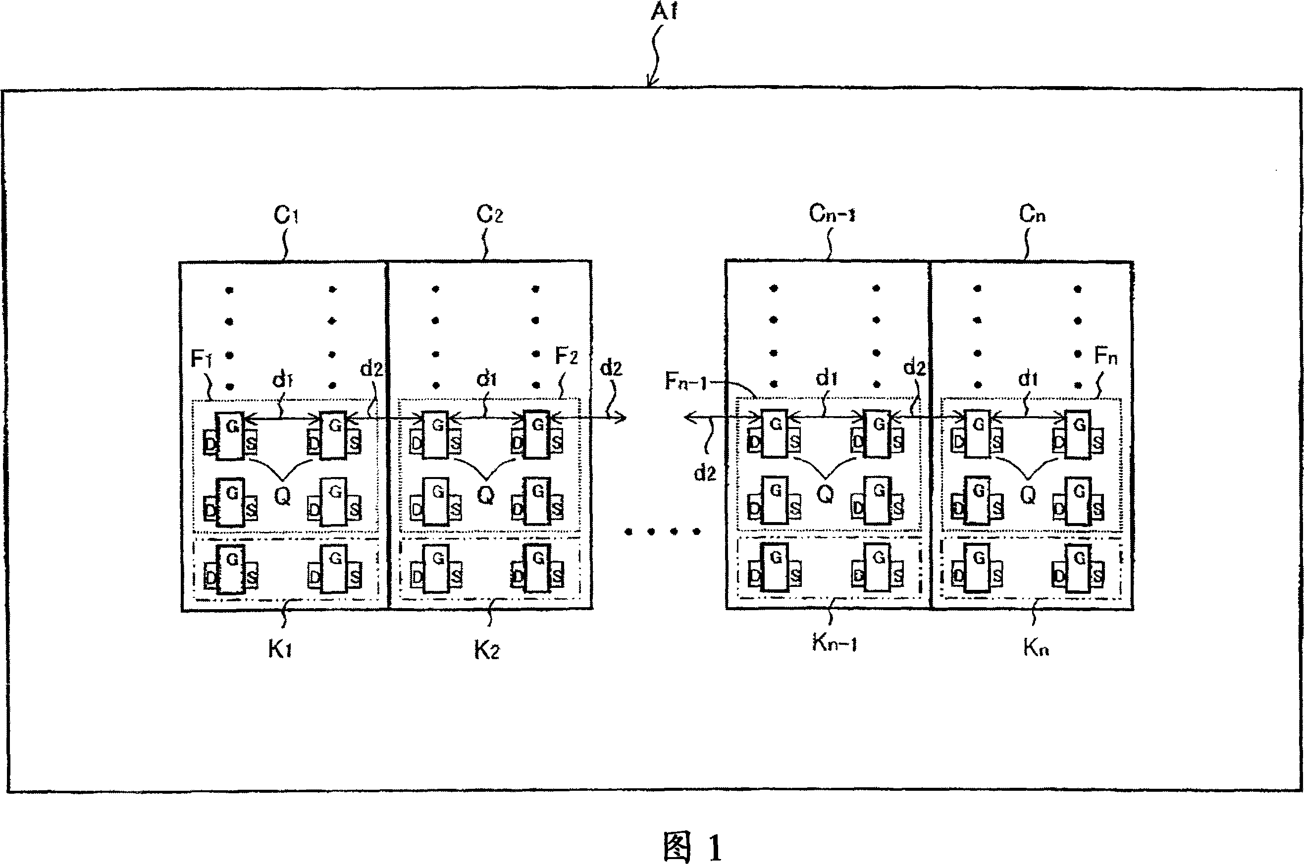
[0046] FIG. 1 is a plan view showing a schematic configuration of a semiconductor device A1 according to a first embodiment of the present invention. In Figure 1, the reference symbol C 1 to C n (wherein n is a natural number not less than 2) are units having the same specifications as each other, and reference symbol F 1 to F n Is the differential amplifier circuit constituting the unit, reference symbol K 1 to K n It is the current mirror circuit that constitutes the unit. Both the differential amplifier circuit and the current mirror circuit are constructed of a transistor pair including a pair of transistors. Reference sign d 1 is the distance between one transistor and the other transistor in the transistor pair (it is strictly speaking the distance from gate edge to gate edge, which will be referred to as "intra-cell distance" hereinafter).
[0047] Arrange multiple cells C at the same pitch 1 to C n , thus forming a unit group, the distance between the transist...
no. 2 example
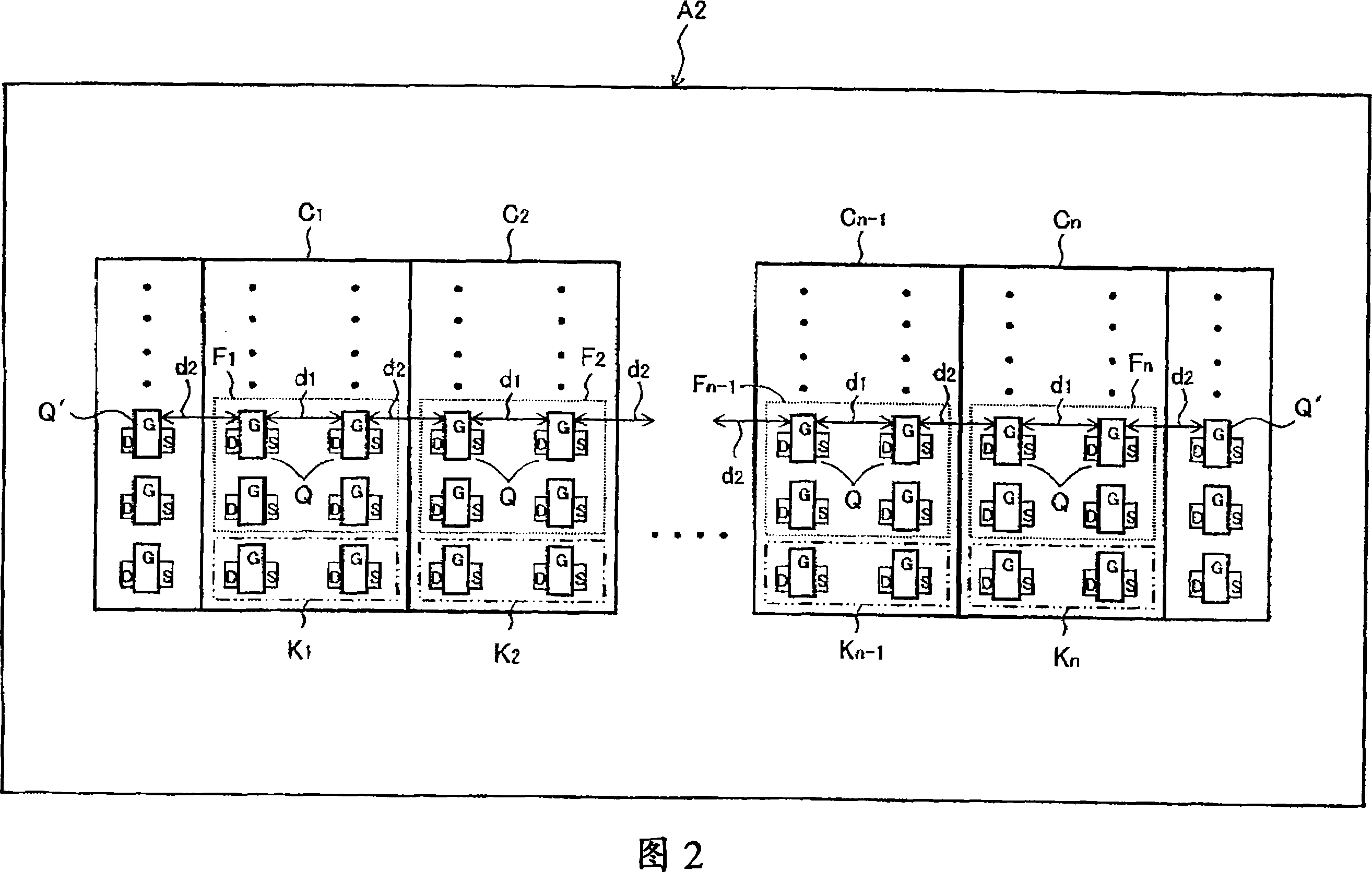
[0060] FIG. 2 is a plan view showing a schematic configuration of a semiconductor device A2 according to a second embodiment of the present invention. In FIG. 2, the same reference numerals as in FIG. 1 of the first embodiment denote the same components. In this embodiment, in addition to the configuration of Figure 1, the units C at both ends of the unit group are 1 and unit C n The dummy transistor Q' is arranged on the outside of the cell arrangement direction. The location of the dummy transistor Q’ is similar to that of the group end cell C located at the edge of the cell group 1 and C n The transistors Q are separated by the intra-cell distance d 1 . That is, the inter-unit distance d 2 Here also equals the intra-element distance d 1 (d 1 = d 2 ). Since other configurations are similar to those of the first embodiment, explanations thereof are omitted.
[0061] According to this embodiment, since the distribution density of transistors becomes uniform througho...
no. 3 example
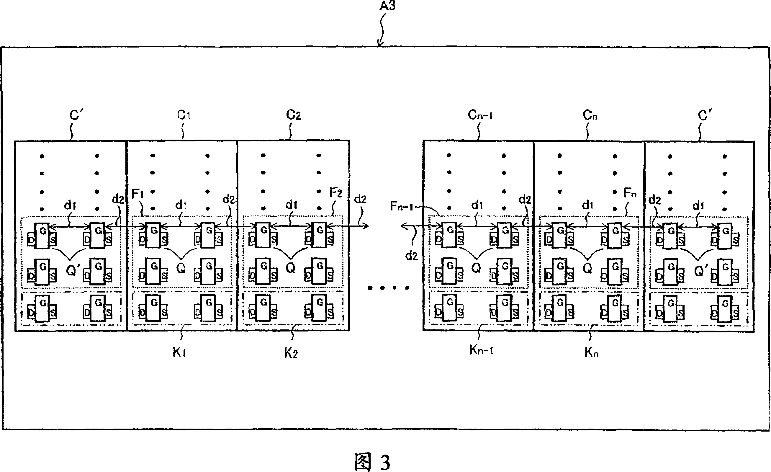
[0063] 3 is a plan view showing a schematic configuration of a semiconductor device A3 according to a third embodiment of the present invention. In FIG. 3 , the same reference numerals as in FIG. 1 of the first embodiment denote the same components. In this embodiment, in addition to the configuration of FIG. 1, the units C located at the edge (both ends) of the unit group 1 and unit C n The dummy cell C' is arranged on the outside of the cell arrangement direction. The size and element pitch of dummy cell C' are the same as those specified in each cell. The placement of internal transistors in dummy cell C’ is similar to that of cell C at the edge of the cell group 1 and C n The transistors Q are separated by an intra-cell distance. That is, the inter-unit distance d 2 Here also equals the intra-element distance d 1 (d 1 = d 2 ). Since other configurations are similar to those of the first embodiment, explanations thereof are omitted.
[0064] According to the pres...
PUM
 Abstract
Description
Claims
Application Information