
Piecewise linearly compensated CMOS bandgap voltage reference

A reference voltage source, piecewise linear technology, applied in the direction of adjusting electrical variables, control/regulation systems, instruments, etc., can solve the problems of complex curvature correction parameter algorithm, large circuit power consumption, chip area and power loss, etc., to achieve High practical value and promotion value, occupying a small chip area, and improving the effect of temperature stability

Inactive Publication Date: 2008-01-09
UNIV OF ELECTRONICS SCI & TECH OF CHINA
View PDF0 Cites 41 Cited by
  • Summary
  • Abstract
  • Description
  • Claims
  • Application Information

AI Technical Summary

Problems solved by technology

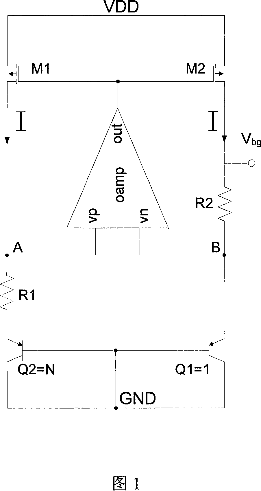
where the exponential curvature compensation through is at V BE Superimpose an exponential function of temperature to achieve the purpose of eliminating high-order terms, but the curvature correction parameter algorithm is complex, the circuit consumes a lot of power and is not flexible, and cannot be realized in a standard CMOS process; the second-order temperature compensation is achieved by adding a single proportional to the square of temperature (PTAT 2 ) term to achieve the elimination of V BE quadratic term, but produces a proportional to the square of temperature (PTAT 2 ) voltage requires a very complex circuit, resulting in significant on-chip area and power loss; linearizing V BE The output voltage of the circuit mentioned in the compensation is very sensitive to the accuracy of the resistance ratio, and a large number of resistance arrays need to be added for fine-tuning, which occupies a large area, and uses a BiCMOS process, and the cost is high; Compensation for the characteristics of temperature changes is limited by the process. Under the same process, it is difficult to improve the performance of the circuit by improving the circuit structure.

Method used


Image

  • Piecewise linearly compensated CMOS bandgap voltage reference
  • Piecewise linearly compensated CMOS bandgap voltage reference
  • Piecewise linearly compensated CMOS bandgap voltage reference

Examples


Embodiment Construction

[0030] The present invention will be further described below in conjunction with the drawings and embodiments.

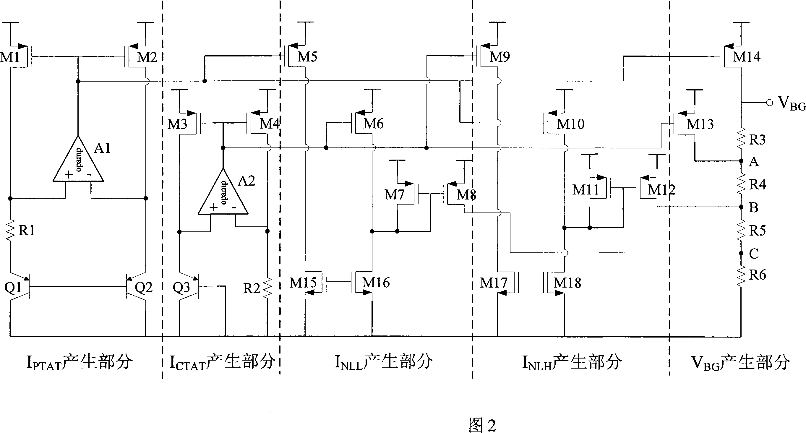
[0031] The bandgap reference voltage source with piecewise linear compensation proposed in the present invention, as shown in Figure 2, is based on the traditional first-order compensated bandgap reference, and will increase two current branches I CL And I CH , And then obtain the high and low temperature compensation voltages, and superimpose them on the first-order compensation voltage to compensate the high temperature and low temperature parts respectively, so as to obtain a more accurate output reference voltage.

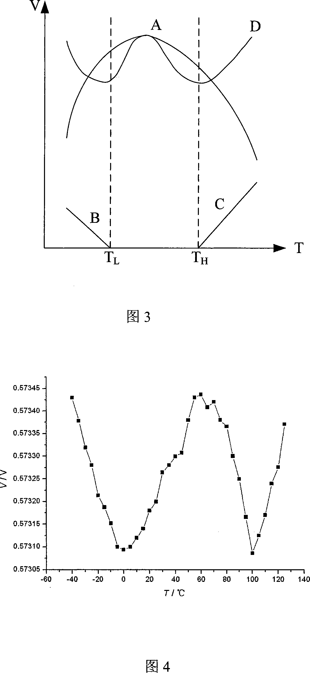
[0032] The basic idea of ​​piecewise linear compensation is shown in Figure 3. In the figure, curve A is the output voltage after first-order compensation, curve B is the low temperature compensation voltage used to compensate the temperature characteristics of A in the low temperature section, and curve C is used for The high temperature compensation vo...


PUM


Abstract

The invention discloses a segmented linear compensated CMOS band gap reference voltage source, characterized in that it comprises IPTAT current generation part, ICTAT current generation part, low temperature segment compensation current ICL generation part and high temperature segment compensation current ICH generation part. On the basis of traditional first-order curvature compensation, it divides the whole temperature range into high, medium and low temperature segments, compensates output voltage in each temperature range respectively and makes the output voltage have multiple local extremum points in the whole temperature range to achieve the segmented compensation purpose, so as to effectively improve the temperature characteristics of output voltage reference, reduce temperature coefficients and improve accuracy of output voltage. Besides, it can change amplitude of output voltage by regulating resistor ratio value, relatively flexible to use. The whole circuit has low power consumption and occupies smaller chip area.

Description

Technical field [0001] The invention relates to a bandgap reference voltage source circuit, in particular to a CMOS bandgap reference voltage source with piecewise linear compensation. Background technique [0002] Generally speaking, the power supply voltage introduced from the outside of the chip has certain fluctuations, and the analog circuit has higher requirements for the stability of the bias voltage. Therefore, in the analog circuit, we generally use a reference voltage source, which will power the power supply. The voltage is converted into a voltage with good voltage stability and temperature stability, which provides a good bias for other parts of the circuit. [0003] The voltage reference circuit is widely used in high-precision analog and digital-analog hybrid circuits, such as readout circuits, high-precision comparators, (A / D, D / A) converters, Voltage regulator, and DC / DC converter, etc. In the digital-to-analog converter, the DAC selects and generates analog outp...

Claims


Application Information

Patent Timeline
IPC IPC(8): G05F3/24
Inventor 吴志明杨鹏蒋亚东吕坚袁凯
Owner UNIV OF ELECTRONICS SCI & TECH OF CHINA
Learn More