
Semiconductor memory device

A conductive type, MOS transistor technology, applied in the field of semiconductor storage devices, can solve the problems of increased standby current, current consumption, etc., and achieve the effects of reducing standby current, reducing GIDL, and reducing voltage difference

Inactive Publication Date: 2008-01-23
NEC ELECTRONICS CORP
View PDF3 Cites 11 Cited by
  • Summary
  • Abstract
  • Description
  • Claims
  • Application Information

AI Technical Summary

Problems solved by technology

[0022] In the above-mentioned Patent Documents 1 and 2, the connection is switched between different potentials at the time of activation and at the time of standby, so that current consumption occurs due to charging / discharging on the connection node at the time of switching the connection
[0023] Therefore, when active-standby switching occurs frequently, the GIDL during standby is reduced, but the charging / discharging current of the connection node is affected, and the standby current increases instead.

Method used


Image

  • Semiconductor memory device
  • Semiconductor memory device
  • Semiconductor memory device

Examples


Embodiment

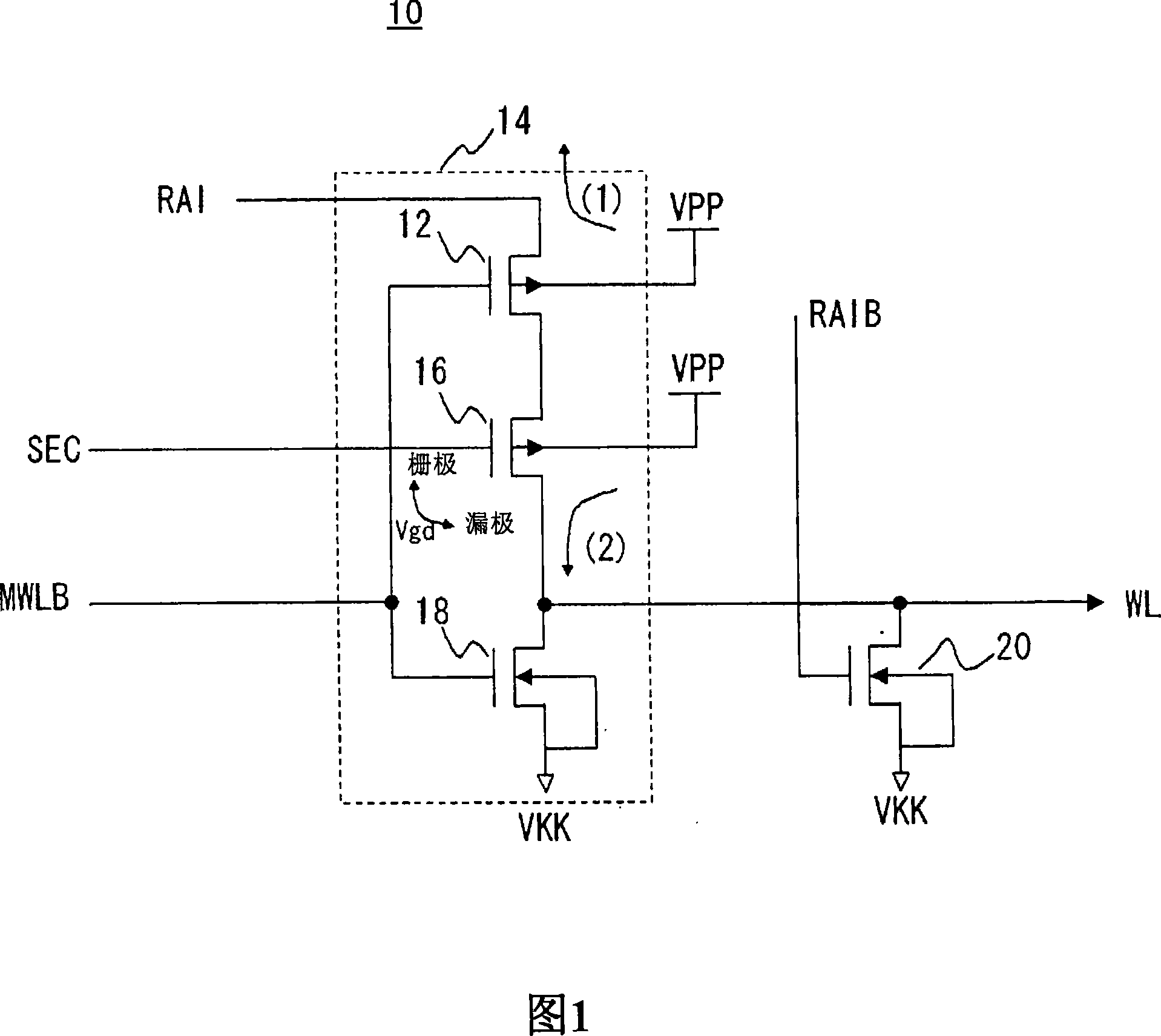
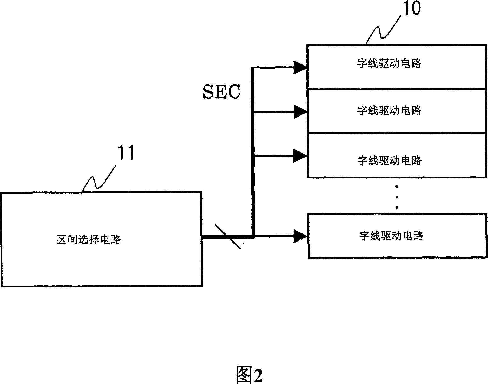
[0049] FIG. 1 is a diagram showing the configuration of a word line driver circuit according to an embodiment of the present invention. As shown in FIG. 1, in the word line driving circuit 10 of the present embodiment, the following signals are input: the main word signal MWLB (the inversion signal of the main word line MWL), the selection period is LOW level, and the non-selection period is HIGH level. Level, supply boost voltage; Sub-word decoding signal RAI, in the selection period of this word line drive circuit 10, is HIGH level (boost voltage), non-selection period is LOW level; RAIB as the inversion signal of RAI ; and a section signal (section signal) SEC signal, the amplitude of which is smaller than that of the main word signal MWLB. The word driver (also referred to as "sub-word driver") 14 includes: a PMOSFET 12 whose source is connected to RAI; an NMOSFET 18 whose source is connected to VKK; and a PMOSFET 16 whose source is connected to the drain of PMOSFET 12 and...


PUM


Abstract

Disclosed is a word line driving circuit which includes a first MOS transistor and a second MOS transistor having mutually different conductivity types and a third MOS transistor of a conductivity type which is the same as that of the first MOS transistor. Gates of the first and second MOS transistors are connected in common for receiving an input signal. Sources of the first and second MOS transistors are connected to a first power supply and a second power supply, respectively. The third MOS transistor is connected between a drain of the first MOS transistor and a drain of the second MOS transistor. A connection node between the drain of the second MOS transistor and a drain of the third MOS transistor is connected to a word line. When the input signal is set to a high level and when the second transistor is turned on, a potential lower than a high level of the input signal is supplied to a gate of the third MOS transistor. A signal with a high level thereof being lower than a high level of the input signal, or a fixed GND potential is supplied to the gate of the third MOS transistor.

Description

technical field [0001] The invention relates to a semiconductor storage device, in particular to a word line drive circuit. Background technique [0002] In recent years, the battery storage time of mobile phone terminals has been required to be longer, and the dynamic memory (which needs to be refreshed to maintain cell data) mounted on mobile phone terminals and the like has also been required to reduce power consumption. In addition, as a dynamic memory mounted on a mobile phone terminal, etc., there are DRAM (Dynamic Random Access Memory) and analog SRAM (Static Random Access Memory). The analog SRAM has a memory core composed of DRAM cells and conforms to the SRAM interface specification. [0003] In particular, it is important to reduce the power consumption (standby current) of the dynamic memory when the dynamic memory is in standby by prolonging the battery retention time in the standby state which occupies most of the use state of the mobile phone terminal. [000...

Claims


Application Information

Patent Timeline
Patent Type & Authority Applications(China)
IPC IPC(8): G11C8/08
CPCG11C11/413G11C11/4085G11C11/40615G11C2211/4067G11C11/406G11C8/08G11C2211/4068
Inventor 宫田昌树
Owner NEC ELECTRONICS CORP
Learn More