Check patentability & draft patents in minutes with Patsnap Eureka AI!

Secondary stack device and its data push and pop methods

A technology of stacking and data, applied in the field of integrated circuits, to achieve the effect of simple circuit structure, convenient control, and cost reduction

Inactive Publication Date: 2011-11-30
SUZHOU HUAXIN MICROELECTRONICS
View PDF1 Cites 0 Cited by
  • Summary
  • Abstract
  • Description
  • Claims
  • Application Information

AI Technical Summary

Problems solved by technology

However, the stack (STACK) circuit implemented by random access memory (RAM) structure is complicated, the control is not easy, and the circuit area is large and the cost is high.

Method used


Image

  • Secondary stack device and its data push and pop methods
  • Secondary stack device and its data push and pop methods
  • Secondary stack device and its data push and pop methods

Examples


Embodiment Construction

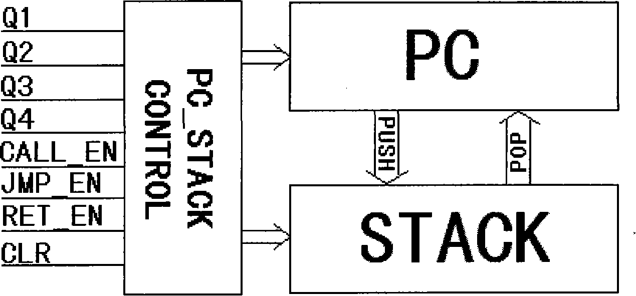
[0031] Such as figure 1 Shown, a kind of two-stage stacking device comprises controller PC STACK CONTROL, bus module PC and two-stage stack register STACK, and bus module PC and two-stage stack register STACK are connected through address bus, and are controlled by controller PC STACK CONTROL Next, push and pop data from the stack.

[0032] The controller PC STACK CONTROL includes eight signal input terminals, four of which are used as the input terminals of the four-phase clock; one input terminal receives the system's subroutine call command enable signal CALL EN, and the subroutine call command enable signal CALL EN It is valid when the subroutine call command is executed; one input terminal receives the jump command enable signal JMP EN of the system, and the jump command enable signal JMP EN is valid when the jump command is executed (including subroutine call command and address jump command ); one input receives the system's subroutine return command enable signal RET...


PUM


Abstract

The invention discloses a two-level stacking device, comprising a controller, a two-level stack register and an address bus module, wherein the controller generates a control signal for controlling the operations of pushing and popping data; the two-level stack The register is used to store the data pushed to the stack; the address bus module is connected with the second-level stack register through the address bus, and is characterized in that the second-level stack register is composed of a plurality of basic units. The invention also discloses a data stacking and stacking method of the two-level stacking device. The beneficial effect of the invention is that the address bus (PC) and the stack (STACK) are combined, and the data push and pop operations of the stack (STACK) are realized by utilizing the characteristics of the 4-phase clock, the circuit structure is simple, the control is convenient, and the circuit area Small, effectively reducing the cost.

Description

technical field [0001] The invention relates to a two-level stacking device in the field of integrated circuits and a data pushing and popping method thereof. Background technique [0002] In the multipoint control unit (MCU) circuit, the stack (STACK) is an indispensable module. The characteristic of the stack is first in, last out, which is the key to subroutine calls. The two-level stack means that two-level subroutine nesting can be realized, that is, the main program can call subroutine 1, subroutine 1 can call subroutine 2, and subroutine 2 cannot call other subroutines. [0003] In the design of the stack, the stack (STACK) is often separated from the address bus (PC), and the stack (STACK) is implemented with a random access memory (RAM) structure. If the address bus (PC) is 10 bits and can address 1K memory space, the second-level stack needs to be implemented with two 10-bit random access memory (RAM) units to store the jump when the subroutine is called twice ...

Claims


Application Information

Patent Timeline
Patent Type & Authority Patents(China)
IPC IPC(8): G06F9/46G06F9/38G06F9/315G06F13/38
Inventor 江猛贾力
Owner SUZHOU HUAXIN MICROELECTRONICS
Features
  • R&D
  • Intellectual Property
  • Life Sciences
  • Materials
  • Tech Scout
  • Unparalleled Data Quality
  • Higher Quality Content
  • 60% Fewer Hallucinations
Learn More