Flip-chip type semiconductor packaging structure and chip bearing member

A technology of flip-chip and packaging structure, which is applied in the direction of semiconductor devices, semiconductor/solid-state device components, electric solid-state devices, etc., which can solve the problems of absorbing thermal stress, inability to solve effectively, and delamination of dielectric layers, etc., to achieve heat absorption Stress, the effect of avoiding uneconomical problems

Inactive Publication Date: 2008-01-30
SILICONWARE PRECISION IND CO LTD
View PDF5 Cites 11 Cited by
  • Summary
  • Abstract
  • Description
  • Claims
  • Application Information

AI Technical Summary

Problems solved by technology

With the low dielectric constant requirements of these dielectric layer materials, the hard and brittle characteristics of the derived dielectric layer materials are more likely to cause delamination of the dielectric layer, which affects the electrical quality of the product.
The reason is mainly due to the inability to effectively solve and absorb the thermal stress generated during the manufacturing process, resulting in the delamination of the inner layer of the chip.
[0006] In addition, referring to FIG. 2, U.S. Patent No. 6,734,567 discloses a flip-chip semiconductor package, which adds a metal ring 24 on the surface of the substrate 21 to prevent the delamination of the flip-chip underfill from extending to the inside of the substrate 21, but This method still cannot prevent the delamination between the flip-chip underfill and the interface between the flip-chip semiconductor chip 20 and the inner layer of the flip-chip semiconductor chip 20
[0007] In view of the aforementioned deficiencies, in order to reduce the thermal stress caused by the difference in coefficient of thermal expansion (CTE), the industry uses flip-chip underfill materials with low Young's modulus to absorb thermal stress, but low Young's modulus A large amount of flip-chip underfill material cannot provide sufficient support strength for the conductive bumps of flip-chip semiconductor chips; Chip underfill, although it can provide high conductive bump support strength, it is easy to cause delamination of flip-chip semiconductor chips due to thermal stress; therefore, it corresponds to the bonding of chips of different sizes and substrates, and different types of chips. When the chip is bonded to the substrate, it takes a lot of time, energy and trials to find the most suitable flip chip underfill material, resulting in an increase in manufacturing time and cost

Method used


Image

  • Flip-chip type semiconductor packaging structure and chip bearing member
  • Flip-chip type semiconductor packaging structure and chip bearing member
  • Flip-chip type semiconductor packaging structure and chip bearing member

Examples


Embodiment Construction

[0045] The features and functions of the present invention will be further described below through specific specific embodiments in conjunction with the accompanying drawings.

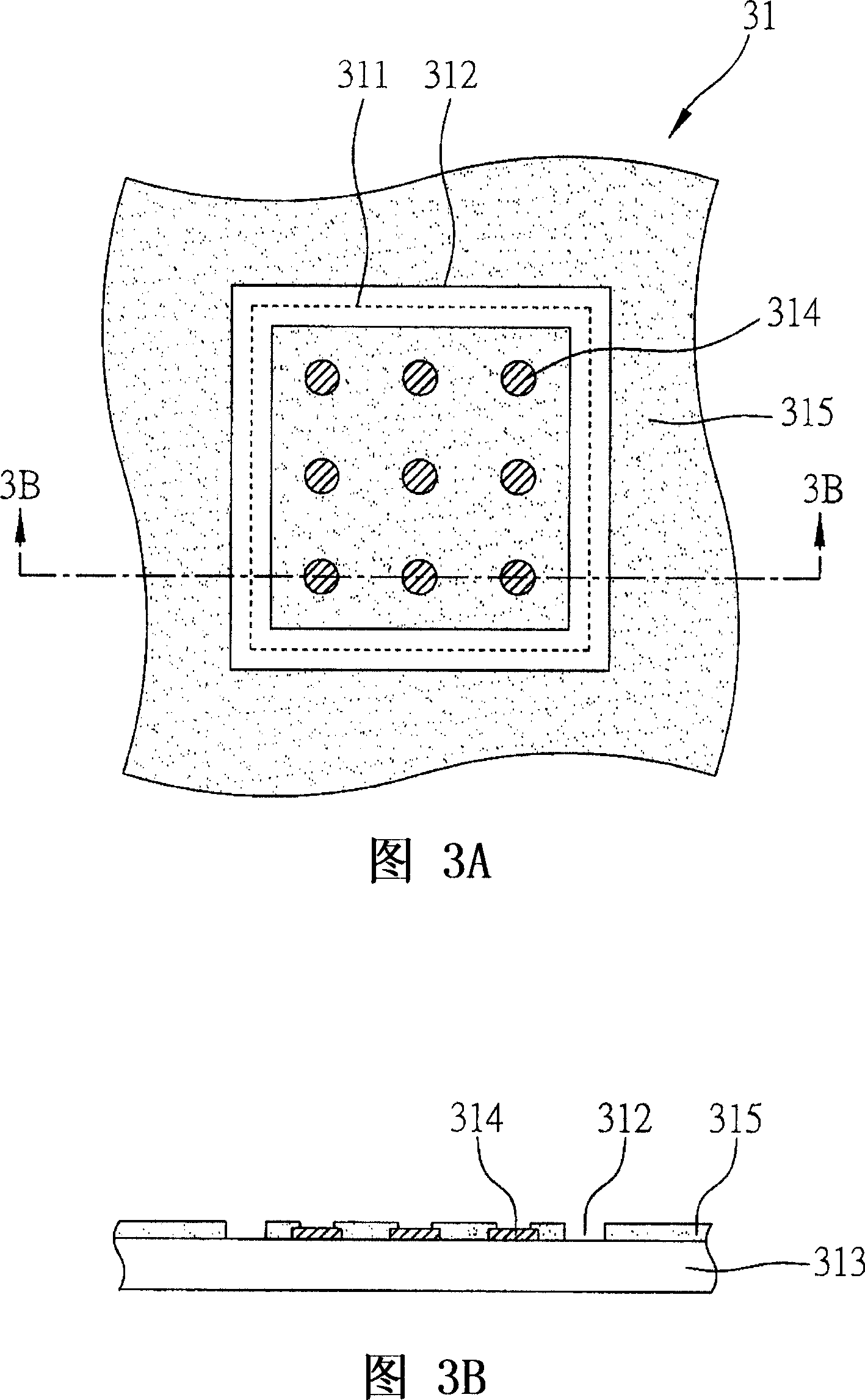
[0046] Referring to FIGS. 3A and 3B , they are schematic diagrams of a chip carrier for a flip-chip semiconductor packaging structure according to the present invention, wherein FIG. 3B is a schematic cross-sectional view corresponding to FIG. 3A .

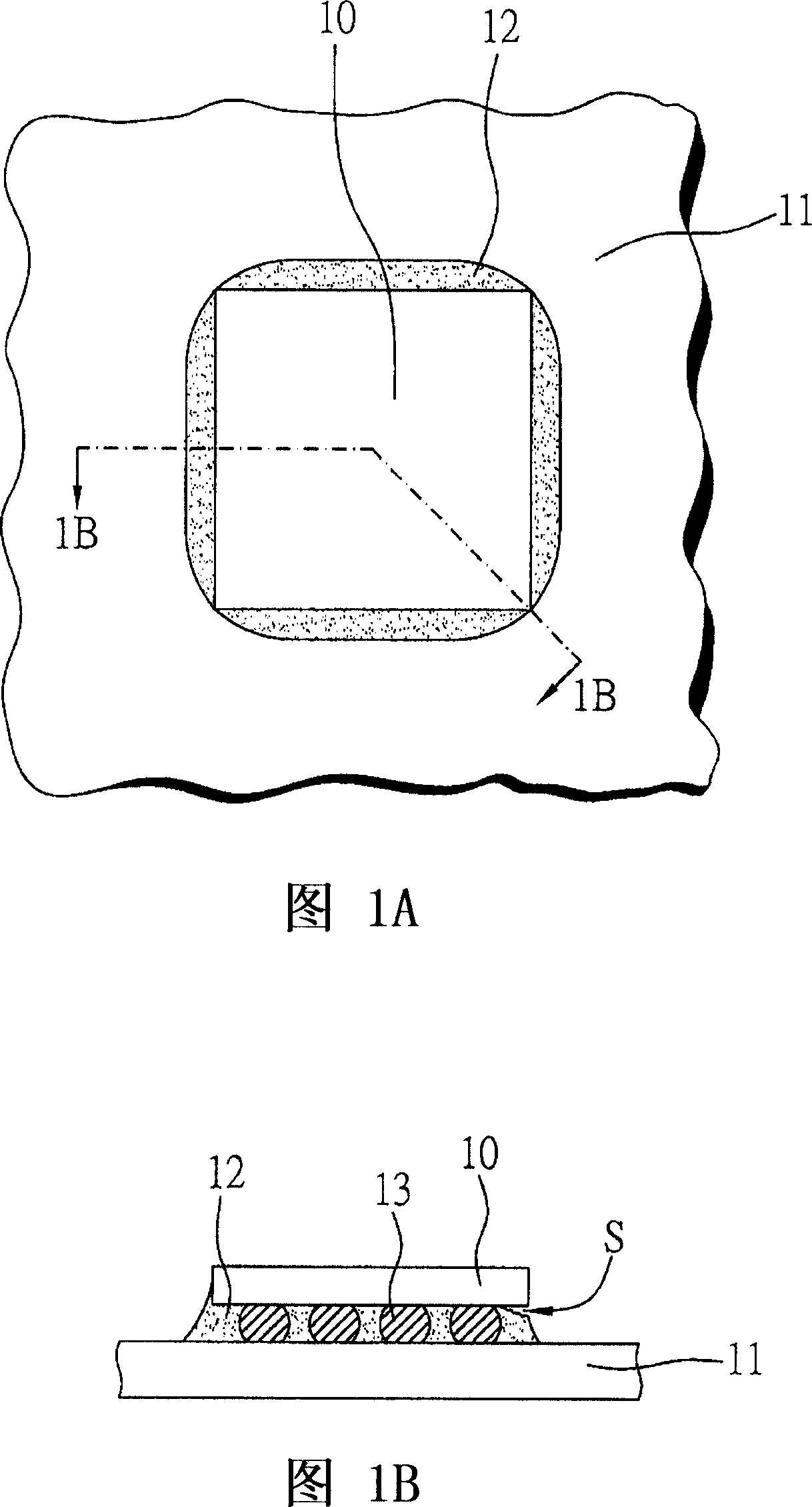
[0047]The chip carrier is a substrate 31, and the substrate 31 includes a body; a chip connection area 311 preset on the surface of the body for connecting flip-chip semiconductor chips; The outer edge of the area 311 is used for filling with low Young's modulus filler.

[0048] The substrate body may for example consist of a core layer 313 , a plurality of solder pads 314 disposed on the surface of the core layer, and a solder resist layer 315 covering the core layer 313 and exposing the solder pads 314 . The solder pad 314 is disposed in the chip placem...


PUM


Abstract

A flip-chip typed semiconductor packaging structure with the related chip carrier is essentially characterized in that an edge of chip linking area of the chip carrier is provided with a groove which can be placed around the edges of the chip linking area or in the corner of the chip linking area, thus soft filler with low young modulus can fill the groove in order to be in connection with the flip-chip typed semiconductor chip in the chip linking area, and the filler with low young modulus absorbs thermal stress in order to avoid delamination between the filling glue at bottom of the chip and the chip.

Description

technical field [0001] The invention relates to a semiconductor package structure and a chip carrier thereof, in particular to a flip-chip semiconductor package structure and a chip carrier thereof. Background technique [0002] Flip-chip semiconductor package is a packaging structure that uses flip-chip for electrical connection. It connects the active surface (Active Surface) of at least one chip through a plurality of conductive bumps (Solder Bumps). ) is electrically connected to the surface of the substrate (Substrate), this design can not only greatly reduce the volume of the package, so that the ratio of the semiconductor chip to the substrate is closer, but also subtract the existing wire (Wire) design, and It can reduce impedance and improve electrical properties, so it has become the mainstream packaging technology for next-generation chips and electronic components. [0003] Referring to FIGS. 1A and 1B, it is a schematic plan view and a cross-sectional view of a...

Claims


Application Information

Patent Timeline
Patent Type & Authority Applications(China)
IPC IPC(8): H01L23/28
CPCH01L2224/16225H01L2224/73204
Inventor 曾渊鳞高迺澔赖正渊王愉博萧承旭
Owner SILICONWARE PRECISION IND CO LTD
Why Eureka
Try Eureka