Sensing type packaging part and manufacturing method thereof

A packaging and sensing technology, applied in semiconductor/solid-state device manufacturing, electrical components, electrical solid-state devices, etc., can solve the problems of film residue, increased process cost and steps, dam structure and substrate delamination, etc.

Inactive Publication Date: 2008-07-30
SILICONWARE PRECISION IND CO LTD
View PDF3 Cites 2 Cited by
  • Summary
  • Abstract
  • Description
  • Claims
  • Application Information

AI Technical Summary

Problems solved by technology

[0006] However, because the film is easy to absorb moisture, it will cause delamination between the dam structure and the substrate, and the use of the film will also increase the cost and steps of the process; moreover, the process of the aforementioned sensing package is mainly in one Substrate modules with multiple substrates arranged in an array are produced in batches, and a plurality of electrical via holes are provided between adjacent substrates. Therefore, after covering the electrical via holes with film, After encapsulation and molding to form the dam structure, as well as placing the crystal and covering the glass, the singulation operation can be performed, and when the cutting tool cuts the film along the adjacent substrate, it is easy to take out the film material together. Cause film residue problem

Method used


Image

  • Sensing type packaging part and manufacturing method thereof
  • Sensing type packaging part and manufacturing method thereof
  • Sensing type packaging part and manufacturing method thereof

Examples


Embodiment Construction

[0038] The implementation of the present invention is described below through specific examples, and those skilled in the art can easily understand other advantages and effects of the present invention from the content disclosed in this specification.

[0039] see Figure 2A FIG. 2F is a schematic diagram of the sensing package and its manufacturing method of the present invention.

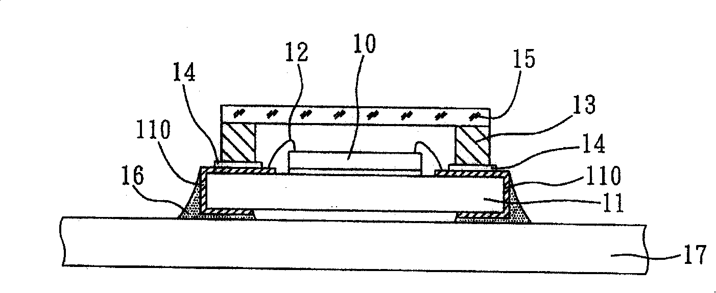
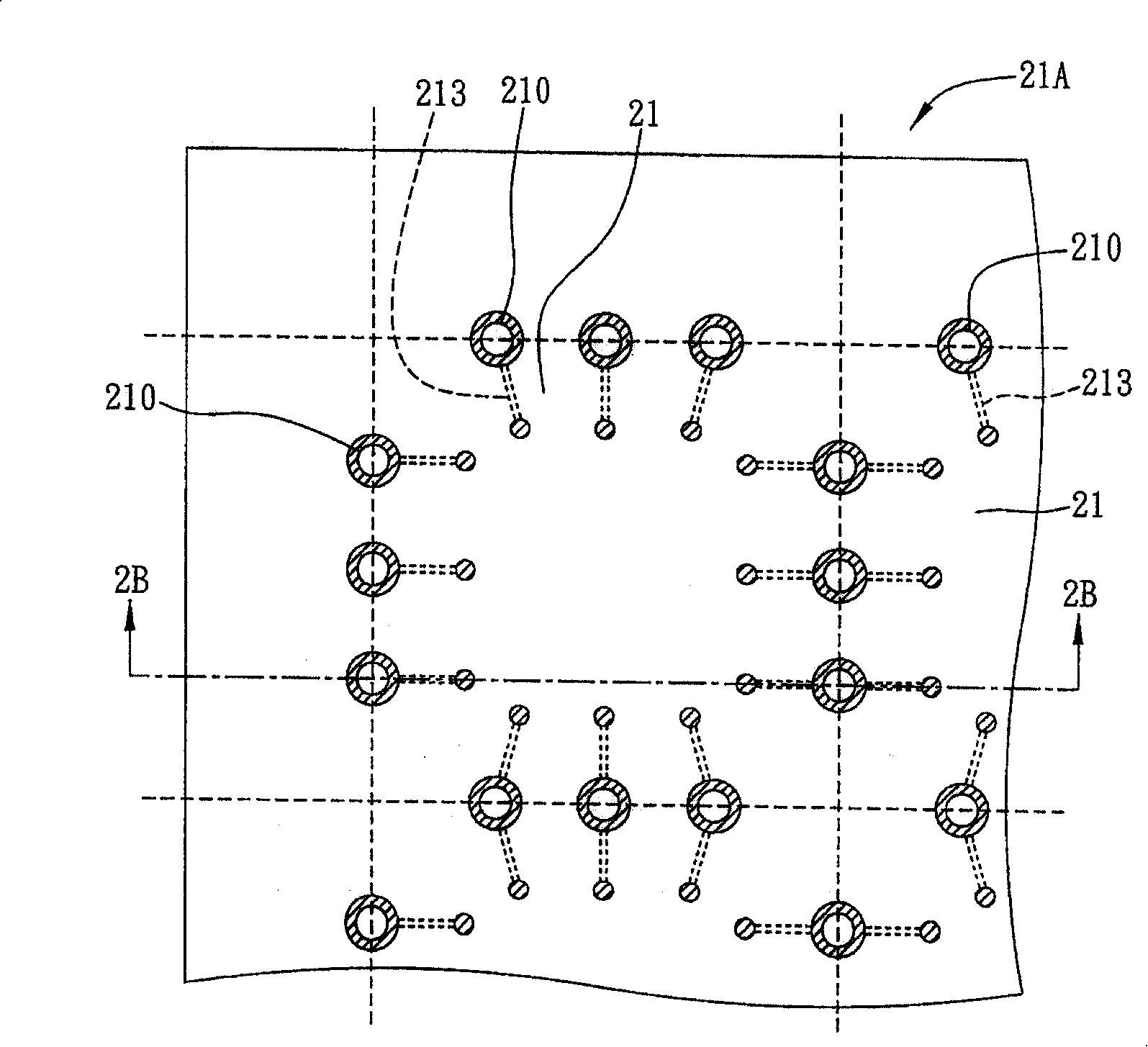
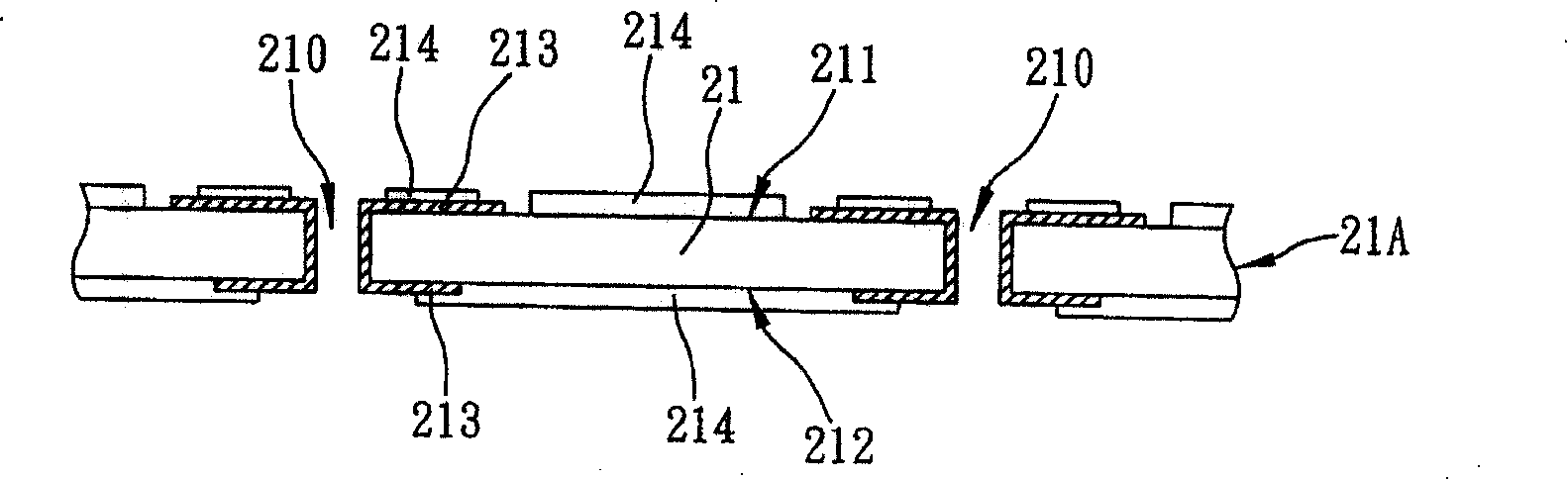
[0040] Such as Figure 2A and Figure 2B shown, where the Figure 2B for correspondence Figure 2A Firstly, a substrate module sheet 21A with a plurality of substrates 21 arranged in an array is provided, and a plurality of electrical via holes 210 are provided between adjacent substrates 21 .

[0041] The substrate 21 has opposite first surface 211 and second surface 212, the substrate first and second surfaces 211, 212 are provided with a plurality of conductive lines 213, and through the electrical conductors formed between the adjacent substrates 21 through holes 210 to electrically conne...


PUM


Abstract

The invention discloses a sensitive packaging part and a manufacturing method thereof. The invention provides a baseplate pattern assembly sheet with a plurality of baseplates which are arranged in array. A plurality of via holes of electric property are arranged between adjacent baseplates, which are filled with and covered with conducting materials. Dam structures covering the conducting materials are formed between adjacent baseplates on the baseplate pattern assembly sheet. The via holes are filled and covered with such conducting materials as soldering tin to prevent the material constituting the dam structure from being drained onto the other surface of the baseplates through via holes. In addition, a tape is not required to be covered on the via holes in advance. The invention eliminates the problem that the tape absorbs moisture which results in separation of the dam structures and the baseplates. Subsequently, sensitive chips can be electrically connected in areas enclosed by the dam structures on the baseplates; transparent units covering the sensitive chips are connected to the dam structures. In the subsequent cutting process, a plurality of sensitive packaging parts are got by means of cutting between the baseplates.

Description

technical field [0001] The invention relates to a semiconductor package and its manufacturing method, in particular to a sensing package and its manufacturing method. Background technique [0002] The traditional image sensor package mainly connects the sensor chip (Sensor chip) on a chip carrier, and electrically connects the sensor chip and the chip carrier through bonding wires, and then A glass is sealed above the sensing chip, so that the image light can be picked up by the sensing chip. In this way, the completed image sensing package can be used by the system factory to integrate on external devices such as printed circuit boards (PCBs) for digital cameras (DSC), digital video cameras (DV), optical mice, etc. , mobile phones and other electronic products. Related technologies can be disclosed in US Patent Nos. 6,262,479, 6,590,269 and 5,962,810. [0003] see figure 1 , to show the sensing package disclosed in US Pat. No. 6,262,479, which forms a dam structure 13 o...

Claims


Application Information

Patent Timeline
IPC IPC(8): H01L21/50H01L27/146H01L23/10H01L23/24H01L31/0203
CPCH01L2224/48091H01L2224/73265H01L2224/97H01L2924/16195H01L2924/00014
Inventor 詹长岳黄建屏张泽文黄致明萧承旭
Owner SILICONWARE PRECISION IND CO LTD
Why Eureka
Try Eureka