Preparation method for multi-element compounds semiconductor single-crystal and growth device thereof

A growth device and compound technology, which is applied in the field of growth device and multi-component compound semiconductor single crystal growth by melt method, can solve the problems of large melt viscosity coefficient, large difference in thermal conductivity between solid and melt, large difference in melting point, etc. Stabilize the solid-liquid interface, achieve flat interface growth, and achieve good crystallization performance

Inactive Publication Date: 2008-02-13
SICHUAN UNIV
View PDF0 Cites 28 Cited by
  • Summary
  • Abstract
  • Description
  • Claims
  • Application Information

AI Technical Summary

Problems solved by technology

The above-mentioned compound semiconductor single crystal growth is difficult, and the Brigdman-Stockarger (B-S method for short) method can generally be used to grow single crystals. However, these compounds have many components, large differences in melting points, large differences in saturated vapor pressure, and are easy to decompose at high temperatures. In addition, the melt is viscous. If the coefficient is large, the second phase will also be precipitated and separated at low temperature; especially during the crystallization process, due to the different segregation coeffi

Method used


Image

  • Preparation method for multi-element compounds semiconductor single-crystal and growth device thereof
  • Preparation method for multi-element compounds semiconductor single-crystal and growth device thereof
  • Preparation method for multi-element compounds semiconductor single-crystal and growth device thereof

Examples


Embodiment 1

[0030] Example 1: Multicomponent Compound Semiconductor Single Crystal Growth Apparatus

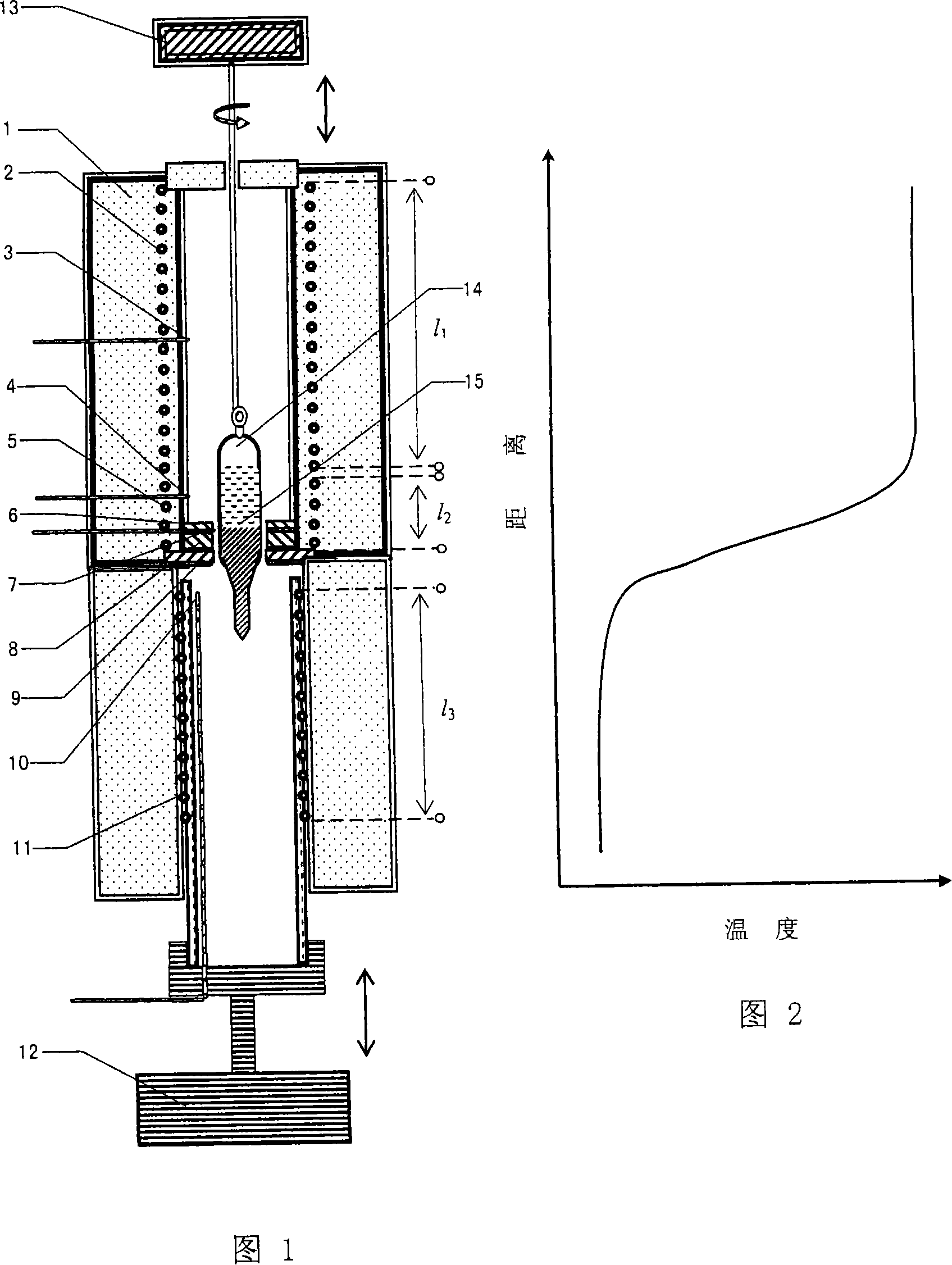
[0031] In this embodiment, the structure of the multi-component compound semiconductor single crystal growth device is shown in FIG. 1, including a furnace body 1, an upper furnace heater, an auxiliary heater, a lower furnace heater, and an upper furnace temperature monitor that are independently heated and temperature-controlled , the lower heat conduction ring 9, the middle heat conduction ring 8, the upper heat preservation and heat insulation ring 6, the lower lifting mechanism 12, and the upper lifting mechanism 13.

[0032] The heating element 2 of the upper furnace heater and the heating element 5 of the auxiliary heater are sequentially installed on the furnace body from top to bottom along the axial direction of the furnace body, and the heating assembly 11 of the lower furnace heater is installed on the lower lifting mechanism 12, Its main body extends into the furnace body and ...

Embodiment 2

[0036] Example 2: AgGaS 2 Preparation of single crystals

[0037] In this embodiment, AgGaS is used 2 The polycrystalline powder was used as the raw material, the quartz crucible was used as the growth vessel, and the crystal growth device described in Example 1 was used. In this device, the auxiliary heater heating element distribution area 1 2 The length is 12cm. The preparation method includes the following process steps in turn:

[0038] ①Clean the crucible

[0039] The cleaning process of the crucible is a combination of comprehensive cleaning and vacuum baking. First, the inner wall of the crucible is soaked and rinsed with tap water, then soaked in hydrofluoric acid for 3 minutes, then rinsed with tap water until neutral, and finally placed in an ultrasonic cleaning tank to oscillate. Clean for 8 minutes and rinse with high-resistance deionized water repeatedly, place the cleaned crucible in a vacuum oven, control the temperature at 130 °C, and bake for 3.5 hours; ...

Embodiment 3

[0048] Example 3: CdGeAs 2 Preparation of single crystals

[0049] In this embodiment, CdGeAs is used 2 The polycrystalline powder was used as the raw material, the quartz crucible was used as the growth vessel, and the crystal growth device described in Example 1 was used. In this device, the auxiliary heater heating element distribution area 1 2 The length is 8cm. The preparation method includes the following process steps in turn:

[0050] ①Clean the crucible

[0051] The cleaning process of the crucible is a combination of comprehensive cleaning and vacuum baking. First, the inner wall of the crucible is soaked and rinsed with tap water, then soaked in hydrofluoric acid for 3 minutes, then rinsed with tap water until neutral, and finally placed in an ultrasonic cleaning tank to oscillate. Wash for 8 minutes and repeatedly rinse with high-resistance deionized water, place the cleaned ampoules in a vacuum oven, control the temperature at 130 °C, and bake for 3.5 hours; ...


PUM


Abstract

A method for preparing a multi-component semiconductor single crystal, the process steps are: (1) cleaning a crucible, (2) charging and degassing and sealing, (3) crystal growth, and (4) annealing and cooling. The single crystal growth device matched with this method includes a movable lower furnace heater and a single crystal growth furnace with an auxiliary heater in the middle, which can flexibly adjust the temperature field in the crystallization temperature gradient area according to the crystallization habit of the multi-component compound, and obtain The narrow temperature zone and large temperature gradient crystallization temperature field distribution required for the growth of compound single crystals maintain the stability of the solid-liquid interface and realize the flat interface growth of single crystals. Using the growth device, various multi-element compound semiconductor single crystals with complete appearance and good crystallization performance can be successfully grown by adopting the crucible descending method.

Description

technical field [0001] The invention belongs to the field of preparation of inorganic single crystal materials, and particularly relates to a method for growing a multicomponent compound semiconductor single crystal by a melt method and a corresponding growth device. technical background [0002] Multiple compound semiconductor single crystals, such as ZnGeP 2 , CdGeAs 2 , AgGaS 2 , AgGaSe 2 , AgGa 1-x In x Se 2 , Cd 1-x Zn x Te et al., due to its excellent infrared nonlinear optical performance or room temperature nuclear radiation detection performance, can be widely used in the field of frequency conversion in the mid-to-far infrared band and room temperature nuclear radiation detection. The above-mentioned compound semiconductor single crystals are difficult to grow. Generally, single crystals can be grown by the Brigdman-Stockarger (B-S method for short) method. However, these compounds have many components, large differences in melting points, large differences...

Claims


Application Information

Patent Timeline
IPC IPC(8): C30B11/00
Inventor 朱世富赵北君何知宇陈观雄
Owner SICHUAN UNIV
Why Eureka
Try Eureka