Isolated gate type bipolar transistor

A bipolar transistor and insulated gate technology, applied in semiconductor devices, electrical components, circuits, etc., can solve problems such as increased operating voltage, increased collector-emitter saturation voltage, and easy breakdown, etc., to achieve Effects of preventing breakdown and reducing on-resistance

Inactive Publication Date: 2008-02-20
SANKEN ELECTRIC CO LTD
View PDF1 Cites 12 Cited by
  • Summary
  • Abstract
  • Description
  • Claims
  • Application Information

AI Technical Summary

Problems solved by technology

[0005] However, there is a problem that when operating at high temperature, the resistance value (Ron) of the N-type base region until the insulated gate bipolar transistor is turned off increases, so the operating voltage becomes large, and the collector-emitter saturation voltage Vce(sat) becomes larger
[0012] However, in the insulated gate bipolar transistor described in the above-mentioned Patent Document 1, there is a problem that breakdown occurs relatively easily.

Method used


Image

  • Isolated gate type bipolar transistor
  • Isolated gate type bipolar transistor

Examples


no. 1 approach

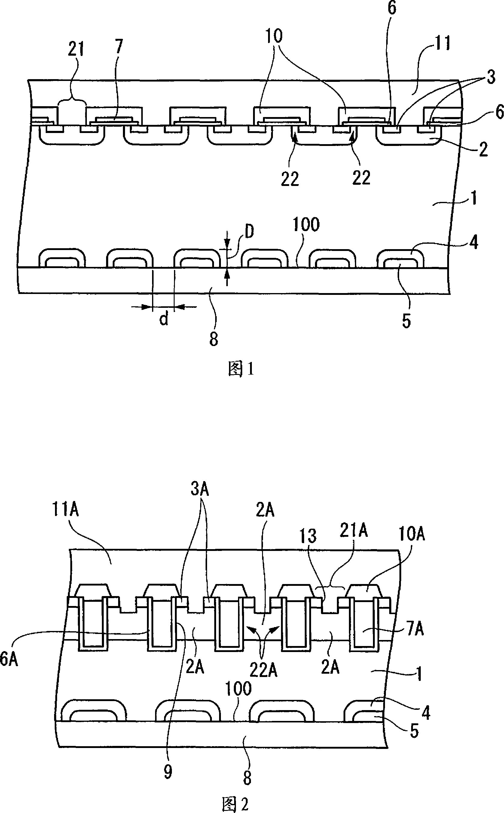
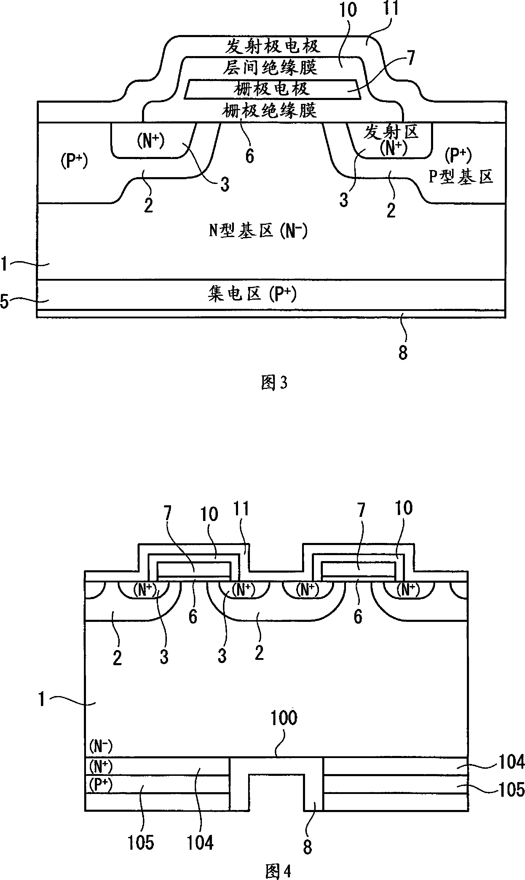
[0032] With reference to the drawings, the insulated gate bipolar transistor according to the first embodiment of the present invention will be described. FIG. 1 is a conceptual diagram showing a cross-sectional structure of an insulated gate bipolar transistor according to a first embodiment of the present invention.

[0033] In FIG. 1, the insulated gate bipolar transistor of this embodiment includes a semiconductor substrate having an N-type base region 1, a P-type base region 2, an emitter region 3, a buffer region 4, and a collector region 5.

[0034] The N-type base region 1 is an N-type semiconductor region (first conductivity type semiconductor region) in which N-type impurities (for example, P: phosphorus, As: arsenic, etc.) are diffused.

[0035] The P-type base region 2 is a P-type semiconductor region in which P-type impurities (for example, B: boron, etc.) are diffused to the top surface (one main surface side) of the N-type base region 1 and formed in stripes.

[003...

no. 2 approach

[0078] Based on the drawings, an insulated gate bipolar transistor according to a second embodiment of the present invention will be described. 2 is a conceptual diagram showing the cross-sectional structure of an insulated gate bipolar transistor according to a second embodiment of the present invention.

[0079] As shown in FIG. 2, the insulated gate bipolar transistor has a trench gate structure formed in the trench, and the buffer area 4 is sandwiched between the periodically formed collector region 5 and the N-type base as one of the characteristics of the present invention. The structure formed between the zones 1 is the same as that of the first embodiment, the same symbols are assigned to the same structures, and the description is omitted.

[0080] As in the first embodiment, the N-type base region 1 is an N-type semiconductor region (first conductivity type semiconductor region) in which N-type impurities are diffused.

[0081] The P-type base region 2A is a P-type semic...


PUM


Abstract

The invention provides an insulated gate type bipolar transistor. The said IGBT comprises a 1st semiconductor region of a 1st conductivity type, a 2nd semiconductor region of a 2nd conductivity type formed in one principal surface side of the 1st semiconductor region, a 3rd semiconductor region of the 1st conductivity type formed in the surface of the 2nd semiconductor region, a 4th semiconductor region of the 1st conductivity type formed in the principal surface side of another side of said 1st semiconductor region with a predetermined distance, a 5th semiconductor region of the 2nd conductivity type formed in the surface in the 4th semiconductor region, a gate electrode formed in said 2nd semiconductor region via an insulator layer, a collector electrode formed in the principal surface side of another side of said 1st semiconductor. The 1st semiconductor region, the 4th semiconductor region, and said 5th semiconductor region are exposed to the principal surface of another side of said semiconductor substrate and each has joined to a collector electrode.

Description

Technical field [0001] The present invention relates to a semiconductor device with a high withstand voltage, and particularly to an insulated gate bipolar transistor (IGBT) used in a power supply circuit and the like. Background technique [0002] In recent years, insulated gate bipolar transistors have been widely used in power circuits and the like because of their excellent characteristics of both a MOSFET with gate insulation and a bipolar transistor with high-current switching characteristics. [0003] As the structure of the insulated gate bipolar transistor, it is known that, as shown in FIG. 3, on the entire surface of the lower side of the N-type base region 1, a P-type set having a conductivity type opposite to that of the N-type base region 1 is formed. An insulated gate bipolar transistor (hereinafter, referred to as a first insulated gate bipolar transistor) formed by the electric region 5. [0004] The above-mentioned first insulated gate bipolar transistor has the...

Claims


Application Information

Patent Timeline
Patent Type & Authority Applications(China)
IPC IPC(8): H01L29/739
Inventor 河野好伸
Owner SANKEN ELECTRIC CO LTD
Why Eureka
Try Eureka