Insulated gate semiconductor device

An insulated gate, semiconductor technology, used in semiconductor devices, electrical components, circuits, etc., can solve problems such as limitations, and achieve the effects of increasing current capacity, reducing device miniaturization, and expanding contact area.

Inactive Publication Date: 2008-02-27
SANYO ELECTRIC CO LTD +1
View PDF1 Cites 5 Cited by
  • Summary
  • Abstract
  • Description
  • Claims
  • Application Information

AI Technical Summary

Problems solved by technology

However, in the above protection circuit in which two MOSFETs Q1 and Q2 are connected in series, there is a limit to this requirement.

Method used


Image

  • Insulated gate semiconductor device
  • Insulated gate semiconductor device
  • Insulated gate semiconductor device

Examples


Embodiment Construction

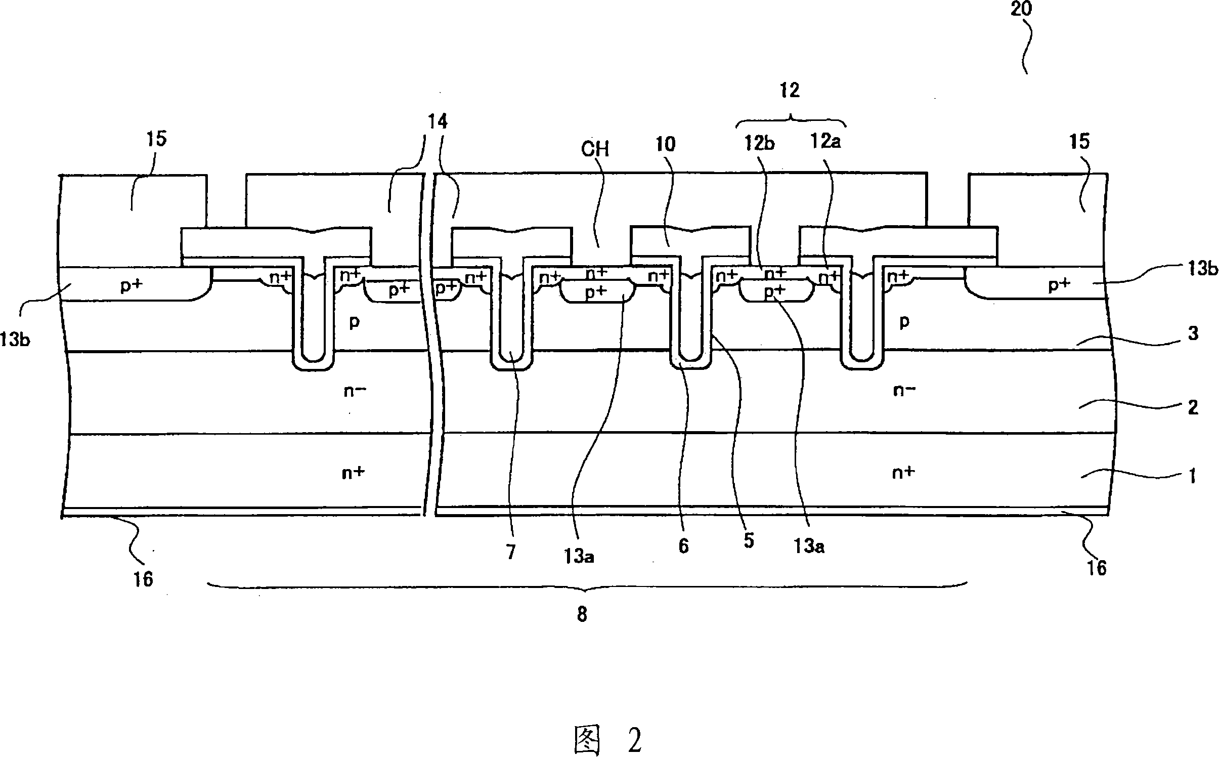
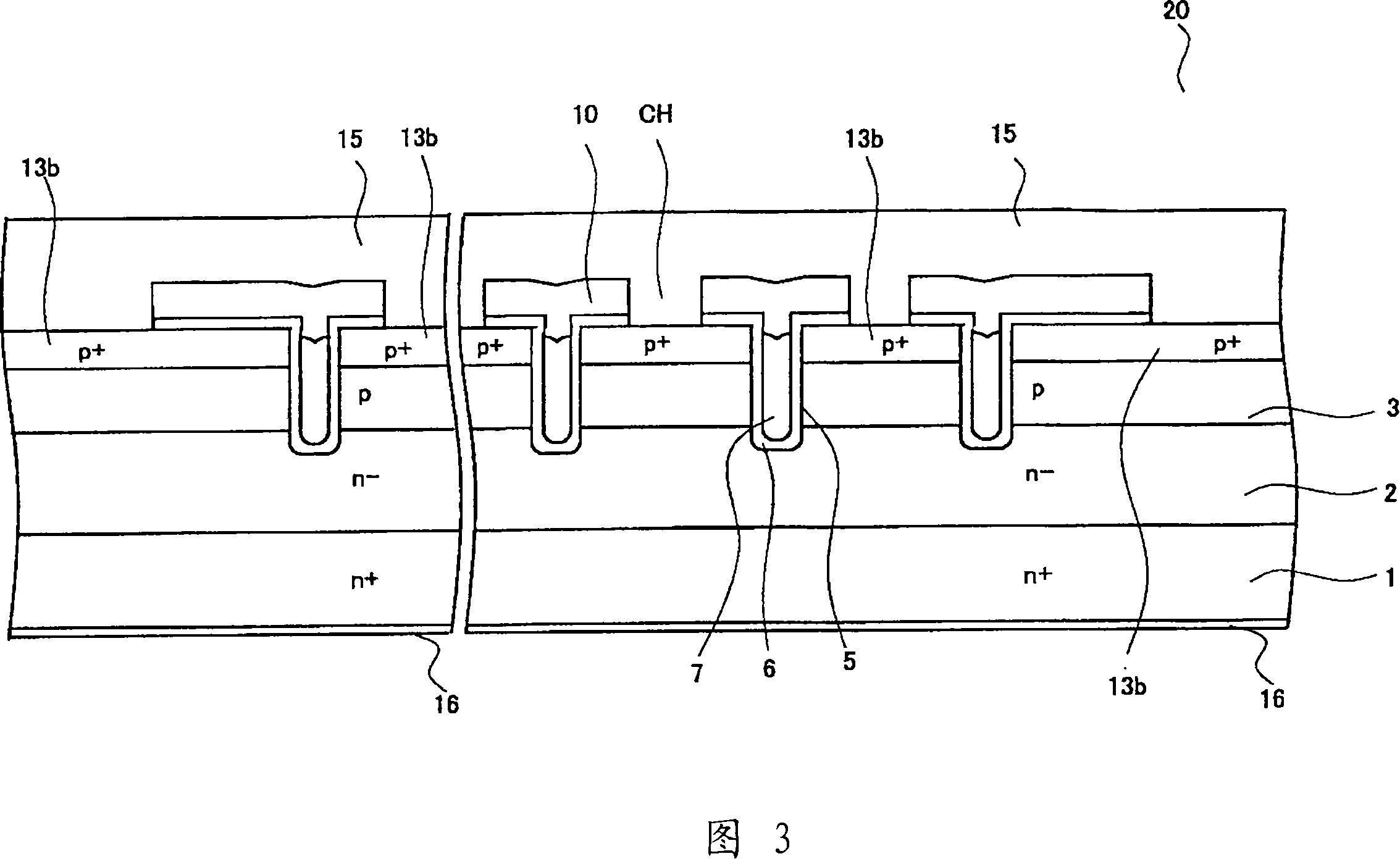
[0078] 1-9, the embodiment of the present invention will be explained by taking an n-channel trench structure MOSFET as an example.

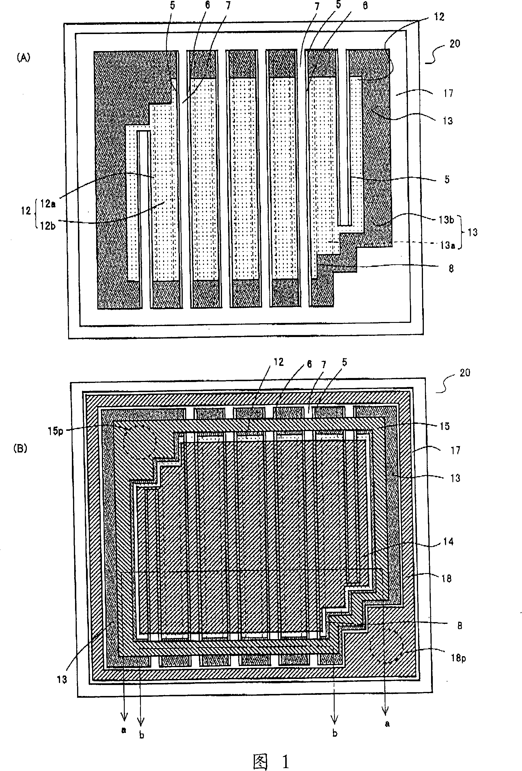
[0079] First, the first embodiment will be described with reference to FIGS. 1 to 8. Fig. 1 is a plan view showing the MOSFET. FIG. 1(A) is a diagram omitting a surface electrode layer and an interlayer insulating film, and FIG. 1(B) is a diagram where a surface electrode layer is arranged.

[0080] MOSFET 20 is composed of semiconductor substrate 1, semiconductor layer 2, channel layer 3, trench 5, gate insulating film 6, gate electrode 7, source region 12, back gate region 13, interlayer insulating film 10, first The electrode layer 14, the second electrode layer 15 and the third electrode layer 16 are constituted.

[0081] On the surface of the substrate where the n- type semiconductor layer is arranged on the n+ type silicon semiconductor substrate, the channel layer 3 as a p-type impurity region is provided. The trench 5 is formed in a pattern ...


PUM


Abstract

The invention provides an insulated gate type semiconductor device. In the existing structure, the source region and the back gate region are in contact with a common source electrode, and the potentials of the source region and the back gate region cannot be controlled separately. Therefore, when such a MOSFET is used as a bidirectional conversion element, two MOSFETs are connected in series, and a control circuit performs on-off of the MOSFET and control of the parasitic diode, which hinders miniaturization of the device. A source region is provided on the entire surface of the active region, a first back gate region is provided under the source region between the trenches, and a second back gate region connected to the first back gate region is provided outside the source region. The first electrode layer in contact with the source region is provided on the entire surface of the active region, and the second electrode layer in contact with the second back gate region is provided on the outer periphery of the first electrode layer. Potentials can be applied to the first electrode layer and the second electrode layer respectively, and control can be performed to prevent backflow caused by parasitic diodes.

Description

Technical field [0001] The present invention relates to an insulated gate semiconductor device, that is, an insulated gate semiconductor device that can perform a bidirectional switching operation by one chip by separating an electrode connected to a back gate region and a source electrode. Background technique [0002] FIG. 10 shows an n-channel MOSFET as an example of a conventional semiconductor device. Fig. 10(A) is a plan view, and Fig. 10(B) is a cross-sectional view taken along line e-e in Fig. 10(A). In addition, in FIG. 10(A), the interlayer insulating film is omitted, and the source electrode is indicated by a broken line. [0003] As shown in FIG. 10(A), trenches 44 are formed in stripes on the surface of the substrate, and source regions 48 and body regions 49 are arranged adjacent to the trenches 44. The trench 44, the source region 48, and the body region 49 extend in the same direction. [0004] As shown in FIG. 10(B), the n-channel type MOSFET is provided with a d...

Claims


Application Information

Patent Timeline
Patent Type & Authority Applications(China)
IPC IPC(8): H01L29/78H01L29/41H01L29/417H01L29/423
CPCH01L29/7813H01L29/1095H01L29/0869H01L29/0865H01L29/0696H01L29/7811
Inventor 石田裕康夏目正
Owner SANYO ELECTRIC CO LTD
Why Eureka
Try Eureka