High voltage tolerance element and producing method thereof

A technology of voltage components and manufacturing methods, applied in the field of electrostatic discharge protection circuits, can solve problems such as failure, damage, and poor coverage of ESD protection circuits, and achieve the effect of reducing leakage current and improving performance

Inactive Publication Date: 2008-03-19
ADVANCED ANALOG TECH INC
View PDF0 Cites 8 Cited by
  • Summary
  • Abstract
  • Description
  • Claims
  • Application Information

AI Technical Summary

Problems solved by technology

3 (a) and 3 (b) leakage current problem is because when forming the double diffused drain structure of FIG. The lightly doped drain 14 is relatively large, and its diffusion degree is relatively strong after the thermal annealing process, resulting in uneven ion concentration of the NB (refer to FIG. 2 ) at the bottom of the heavily doped drain 13, that is, the The lightly doped drain 14 has poor coverage for the bottom NB, so that when the HVNMOS transistor 1 withstands a VDS greater than 12V, the following situations occur: (1) hot carrier effect (hot carrier effect) lead to body current I sub High leakage current (refer to Fig. 3(a) and 3(b)): and (2) said HVNMOS transistor 1 has obvious leakage current on its drain side even when it is turned off (refer to Fig. 7 Curve F)
When the HVNMOS transistor 1 is used in the ESD protection circuit, because the ion concentration uniformity of the bottom NB is not good, when an electrostatic discharge pulse occurs, it will first cause damage to the bottom NB, and then cause the ESD protection circuit fail

Method used


Image

  • High voltage tolerance element and producing method thereof
  • High voltage tolerance element and producing method thereof
  • High voltage tolerance element and producing method thereof

Examples


Embodiment Construction

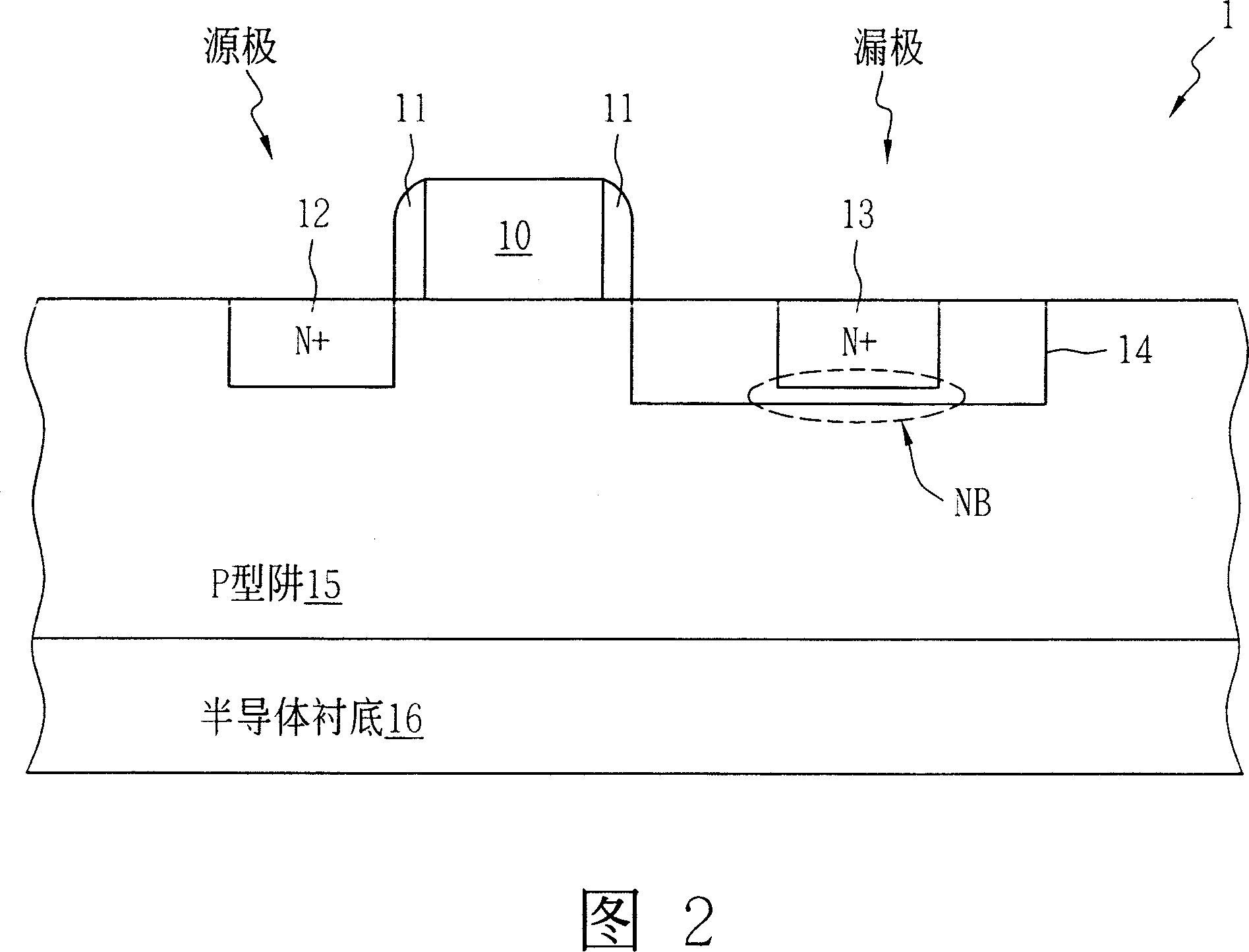
[0019]FIG. 4 is a schematic cross-sectional view of the structure of the high voltage resistant element 2 of the present invention. The high voltage device 2 includes a semiconductor substrate 27 and a gate 20 disposed between two spacers 21 . The semiconductor substrate 27 includes a P-type well region 26, an N-type second doped region 22, an N-type third doped region 23, and an N-type third doped region surrounding the N-type third doped region 23. Four doped regions 24 and an N-type fifth doped region 25 surrounding the N-type third doped region 23 . The gate 20 is used to control the conduction between the N-type second doped region 22 and the N-type third doped region 23 . The length L2 of the N-type fourth doped region 24 is greater than the length L1 of the N-type fifth doped region 25, and the depth D1 of the N-type fifth doped region 25 is greater than the N-type fourth doped region 25. The depth D2 of the impurity region 24. Therefore, the N-type fifth doped regio...


PUM


Abstract

The invention discloses a high-voltage resistant element which comprises a semi-conductive substrate and a gate electrode. The semi-conductive substrate comprises a first doping zone with a first conduction type, a second doping zone with a second conduction type, a third doping zone with a second conduction type, a fourth doping zone surrounding the third doping zone and with a second conduction type, and a fifth doping zone surrounding the third doping zone and with a second conduction type. The gate electrode is adjacently equipped between two clearance walls, and divides the second doping zone from the third doping zone to control the communication between the second doping zone and the third doping zone. The high-voltage resistant element utilizes the fifth doping zone to surround the third doping zone, so as to strengthen the encapsulation of the third doping zone, improve the uniformity of ion concentration at the bottom of the third doping zone, and reduce the drain current thereof.

Description

technical field [0001] The present invention relates to a high voltage resistant element and its manufacturing method, especially to a high voltage resistant metal oxide semiconductor transistor (High Voltage Metal-Oxide-Semiconductor Transistor: HVMOS transistor) and its manufacturing method, the high voltage resistant metal Oxide semiconductor transistors are particularly suitable for protection circuits against electrostatic discharge (ESD). Background technique [0002] In the manufacture and use of integrated circuits (ICs), ESD problems are often encountered. With the increasing demand for high computing speed and wireless broadband communication product ICs, and the current IC technology is rapidly entering 80 nanometers or even below 65 nanometers, the internal components of ICs are very small, so they are easily damaged by instantaneous electrostatic discharge . Therefore, ESD has a great impact on the quality of IC, and with the continuous improvement of IC techn...

Claims


Application Information

Patent Timeline
Patent Type & Authority Applications(China)
IPC IPC(8): H01L29/78H01L27/04H01L21/336H01L21/822
Inventor 方振宇杨盛渊陈维忠
Owner ADVANCED ANALOG TECH INC
Why Eureka
Try Eureka