Wafer test card over current protection method and related wafer test system

A chip testing and overcurrent technology, applied in semiconductor/solid-state device testing/measurement, measuring electricity, measuring electrical variables, etc., can solve problems such as test card burnout, probe damage, and test system failure to detect short-circuit conditions, etc., to achieve The effect of preventing damage

Inactive Publication Date: 2008-03-26
SEMICON MFG INT (SHANGHAI) CORP
View PDF0 Cites 15 Cited by
  • Summary
  • Abstract
  • Description
  • Claims
  • Application Information

AI Technical Summary

Problems solved by technology

However, since the first-stage test does not include power-to-power DC detection, when a wafer with multiple power contact pads has a power-to-power short circuit, the test system cannot detect the short circuit condition.
In the subsequent test, as the test voltage increases, the potential difference between the two contact pads will generate a strong current on the probe, which will cause damage to the probe and burn out of the test card

Method used


Image

  • Wafer test card over current protection method and related wafer test system

Examples


Embodiment Construction

[0014] The overcurrent protection method of the chip test card and the corresponding chip test system of the present invention will be further described in detail below.

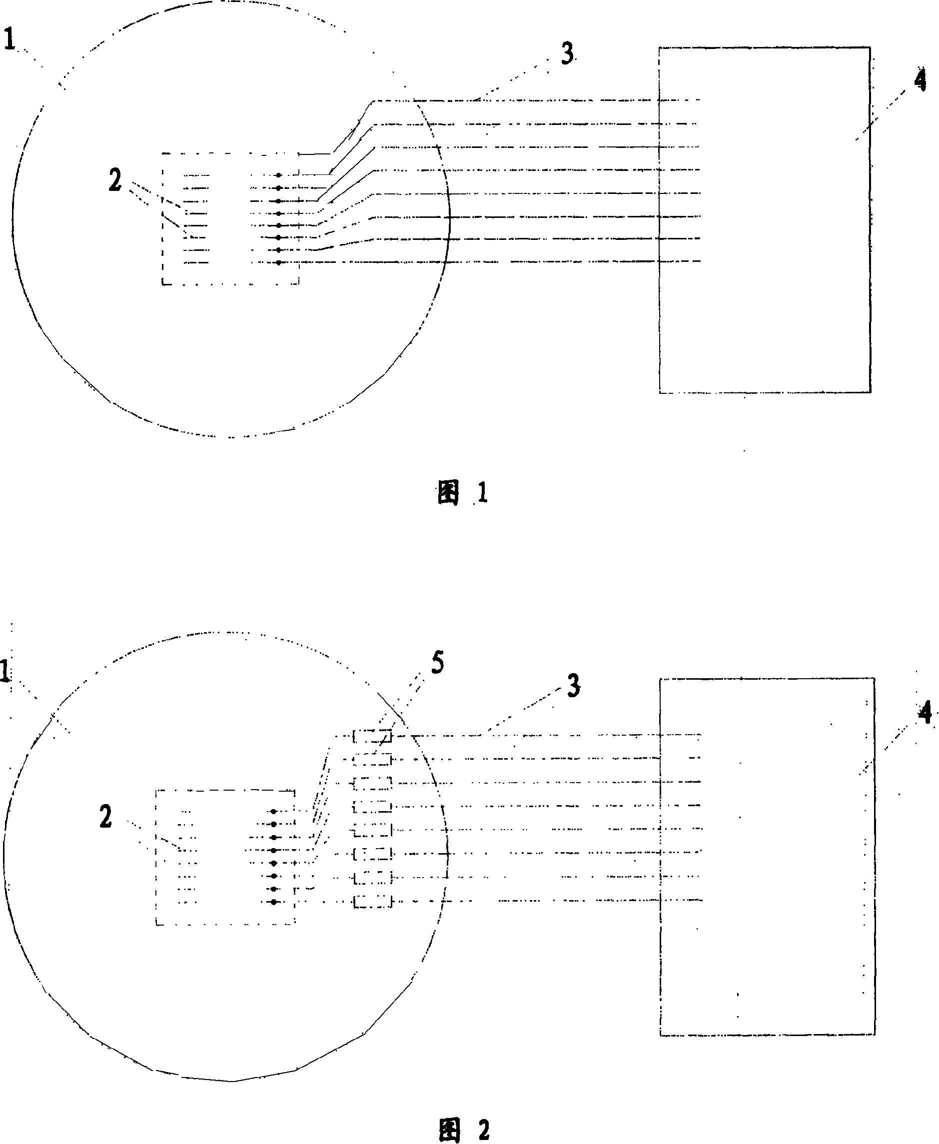
[0015] As shown in Figure 2, compared with the existing system, the wafer test system of the present invention adds an overcurrent protection element 5 between the probe 2 and the lead 3, and this protection element 5 can be selected from a fuse or a current limiting element, The material, length, cross-sectional area of ​​the fuse and the parameter value of the current-limiting element can be set according to the safe current that the probe and the test card can withstand. During the wafer testing process, the current on the wafer flows from the probe 2 through the test card 1 , passes through the protection element 5 and the lead wire 3 , and then flows into the test machine 4 . When a certain contact pad on the chip causes the current flowing through the probe 2 to exceed a safe value due to a short circu...


PUM


Abstract

A kind of overcurrent protection method of the wafer test card and the wafer test system which has the overcurrent protection component. The exist wafer test system has the problem that the high current is short of protecting because of the fault that the butt contact short or other fault. The overcurrent protection method of the wafer test card in this invention includes the following steps: provides a wafer test card, the said wafer test card has several probes, one end of the said probes connects a test machine by down-lead; an overcurrent protection component is connected in series between the said probe and the lead; makes the other end of the said probe contacts with one tested wafer to do wafer test. Uses the overcurrent protection method and wafer test system in this invention can avoid the high current destroying the wafer test card effectively, it can also shows the position of the fault fast, expressly, so it provides convenience to the subsequent work.

Description

technical field [0001] The invention relates to a wafer test method and a test system, in particular to an overcurrent protection method for a wafer test card and a wafer test system with an overcurrent protection element. Background technique [0002] Wafer testing is the process of testing the electrical characteristics of each chip on the wafer to detect and eliminate unqualified chips on the wafer. FIG. 1 is a schematic structural diagram of an existing wafer test system, which mainly consists of a wafer test card 1 , probes 2 , leads 3 and a test machine 4 . When performing a wafer test, the probe 2 of the wafer test card 1 is used to contact the contact pad (pad) on the wafer to form an electrical contact, and then the test signal measured by the probe 2 is sent to the test machine through the lead 3 4. Analyze and judge, so as to obtain the electrical characteristic test results of each chip on the wafer. [0003] The general chip testing process is divided into sev...

Claims


Application Information

Patent Timeline
Patent Type & Authority Applications(China)
IPC IPC(8): G01R1/02G01R1/073G01R1/067G01R31/00G01R31/26G01R31/28H01L21/66
Inventor 常建光
Owner SEMICON MFG INT (SHANGHAI) CORP
Why Eureka
Try Eureka