Chip packaged fixed focus focusing-free imaging module processing method

A technology for chip packaging and camera modules, which is applied in installation, radiation control devices, and printed circuits connected with non-printed electrical components. Achieve the effect of saving product testing equipment and man-hours, improving production efficiency, and improving quality consistency

Inactive Publication Date: 2008-03-26
无锡凯尔科技有限公司
View PDF0 Cites 24 Cited by
  • Summary
  • Abstract
  • Description
  • Claims
  • Application Information

AI Technical Summary

Problems solved by technology

[0006] In the entire manufacturing process, the focusing and dispensing process is the

Method used


Image

  • Chip packaged fixed focus focusing-free imaging module processing method
  • Chip packaged fixed focus focusing-free imaging module processing method
  • Chip packaged fixed focus focusing-free imaging module processing method

Examples


Embodiment Construction

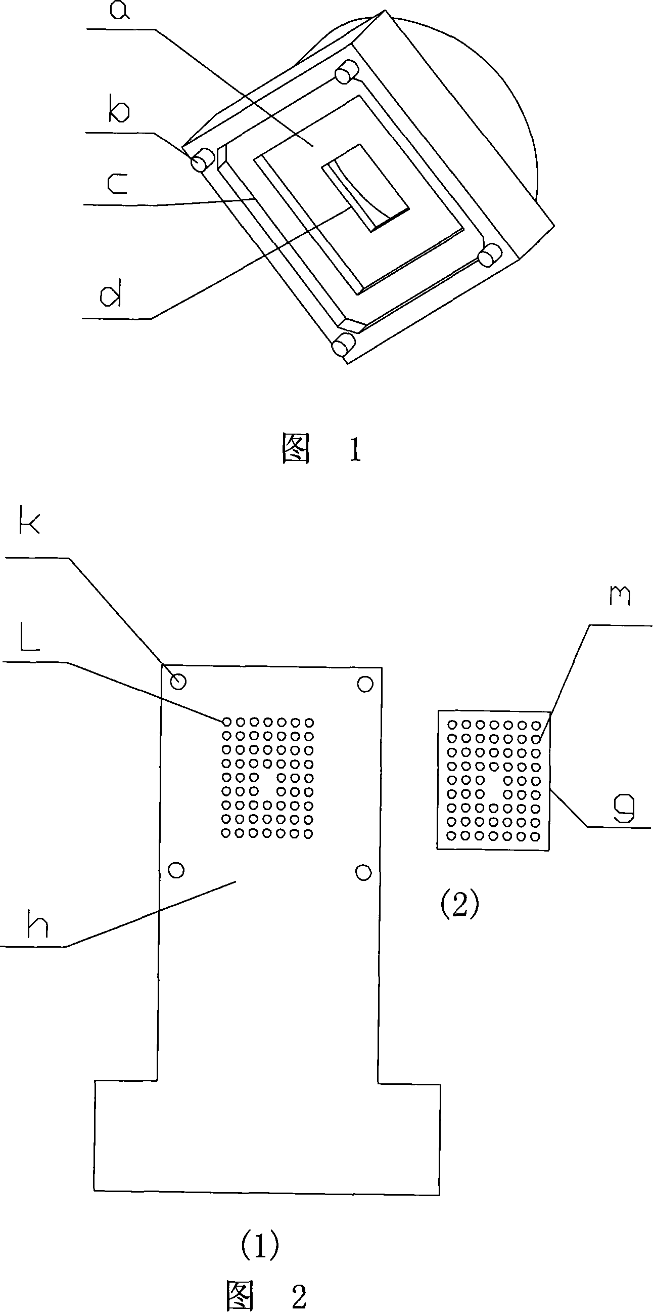
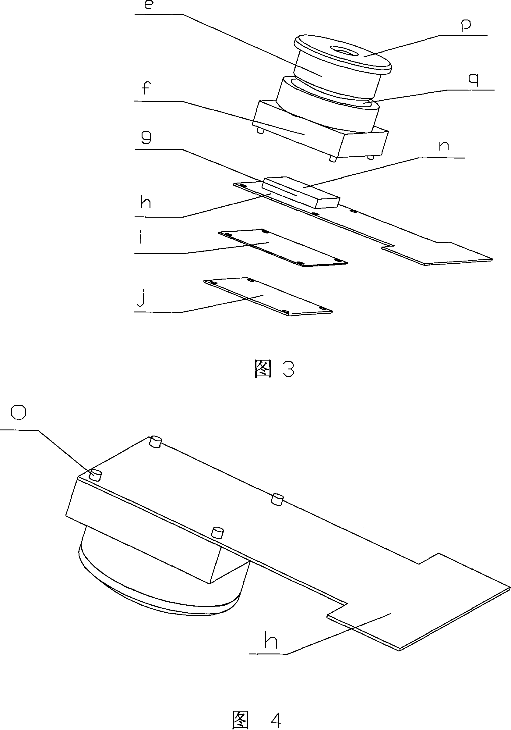
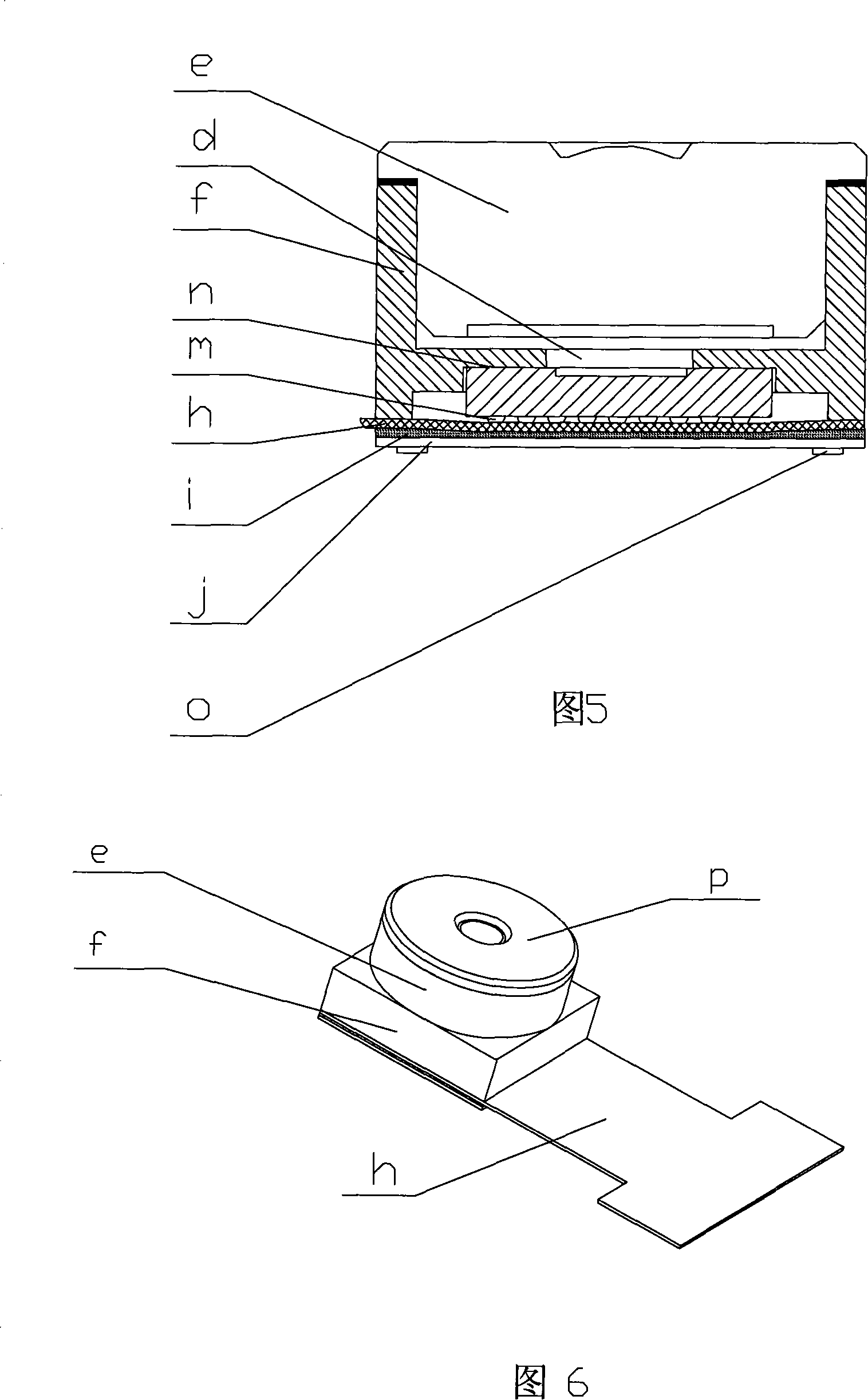
[0029] 1. Prepare lens e: Lens e is wrapped with several lenses inside a plastic shell. Ordinary lens e has threads on the outside, and lens mount f also has threads on the inside. Lens e is screwed in the lens mount f. No need to focus now. The connection between the lens e and the lens holder f is a universal tight-fitting and pressing method. They are pressed together by interference fit. The differences between the lenses are corrected by molds or compensation methods to ensure that the resolution of each lens e is within ± Within 10% error. The lens e has no thread on the outside.

[0030] 2. Prepare the mirror holder f: the bottom surface of the mirror holder f has a positioning surface groove a, and the plane size of the positioning surface groove a is 0.2-0.5mm larger than the image sensor g, so that the image sensor g can be embedded inside, and the image sensor The top of g is just in close contact with the positioning surface groove a of the mirror base f, and the ...


PUM

PropertyMeasurementUnit
Thicknessaaaaaaaaaa

Abstract

This invention relates to the preparation method of the mobile phone, said concretely that it is a kind of chip encapsulation fixed focus mobile telephone image mould process method. According to the technology project provided by the specification, the chip encapsulation fixed focus mobile telephone image mould process method includes: A, compression: compresses the column surface p in the head of camera e and the mounting hole q of the microscope f by interference mating; B, pasting: pastes the image sensor n and device in soft circuit board h; C, joint locating: joints and locates locator surface slot plane of the microscope f and the surface n of image sensor g; D, bonding: pastes the microscope f and the soft circuit board h by adhesive; E, paste double glue: paste soft double glue I in the back camera lens of the soft circuit board h; F, sheet steel bonding, bonds the reinforcing sheet steel j and the back of the soft circuit board h by double glue I; G, hot driving: rivets the locator pole o of the microscope f and the reinforcing sheet steel j by rivet hot machine. This invention can save equipment investment and labor and product cost, improve the quality consistency and product effect of the fixed focus mould.

Description

technical field [0001] The invention relates to a production method of a mobile phone, in particular to a method for processing a chip-packaged fixed-focus mobile phone camera module. Background technique [0002] The full name of CSP is Chip Scale Package, which means chip-level packaging. As a new generation of chip packaging technology, its performance has been improved on the basis of BGA and TSOP. CSP packaging can make the ratio of chip area to package area exceed 1:1.14, which is quite close to the ideal situation of 1:1, and the absolute size is only 32 square millimeters, about 1 / 3 of ordinary BGA, which is only equivalent to TSOP memory chips 1 / 6 of the area. Compared with the BGA package, the CSP package can increase the storage capacity by three times in the same space. The CSP package memory is not only small in size, but also thinner. The most effective heat dissipation path from the metal substrate to the heat sink is only 0.2mm, which greatly improves the ...

Claims


Application Information

Patent Timeline
IPC IPC(8): G02B7/02H05K1/18H01L23/02H01L27/146
Inventor 丁建宏王宁莉邓丹
Owner 无锡凯尔科技有限公司
Why Eureka
Try Eureka