Ultrafast-laser optical chip array processing system and method

An ultra-fast laser and processing system technology, applied to laser welding equipment, metal processing equipment, manufacturing tools, etc., can solve the problems of difficult processing, low processing efficiency, and low production efficiency, and achieve low processing environment requirements and high processing efficiency. Simple equipment and good quality consistency

Inactive Publication Date: 2017-09-26
HUBEI UNIV OF TECH
View PDF9 Cites 10 Cited by
  • Summary
  • Abstract
  • Description
  • Claims
  • Application Information

AI Technical Summary

Problems solved by technology

[0003] At present, the processing of optical chips has problems such as complex processing procedures, high processing difficulty, and low processing efficiency. Traditional processing methods such as chemical etching and mechanical processing have high requirements for operators. The processing quality and its dependence on technical proficiency of the operator
However, using such as electron beam processing, there is a need to maintain a vacuum state in the processing environment, which greatly increases production costs
Laser processing technology is an ideal processing method at present, but the problem of its low production efficiency has been plagued by the realization of large-scale industrial production.

Method used


Image

  • Ultrafast-laser optical chip array processing system and method
  • Ultrafast-laser optical chip array processing system and method

Examples


Embodiment Construction

[0029] The ultrafast laser optical chip array processing system and method of the present invention will be further described below in conjunction with the accompanying drawings and embodiments.

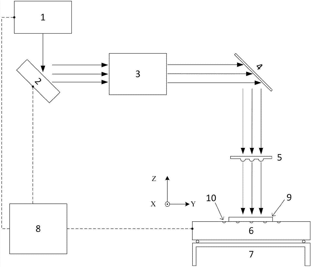
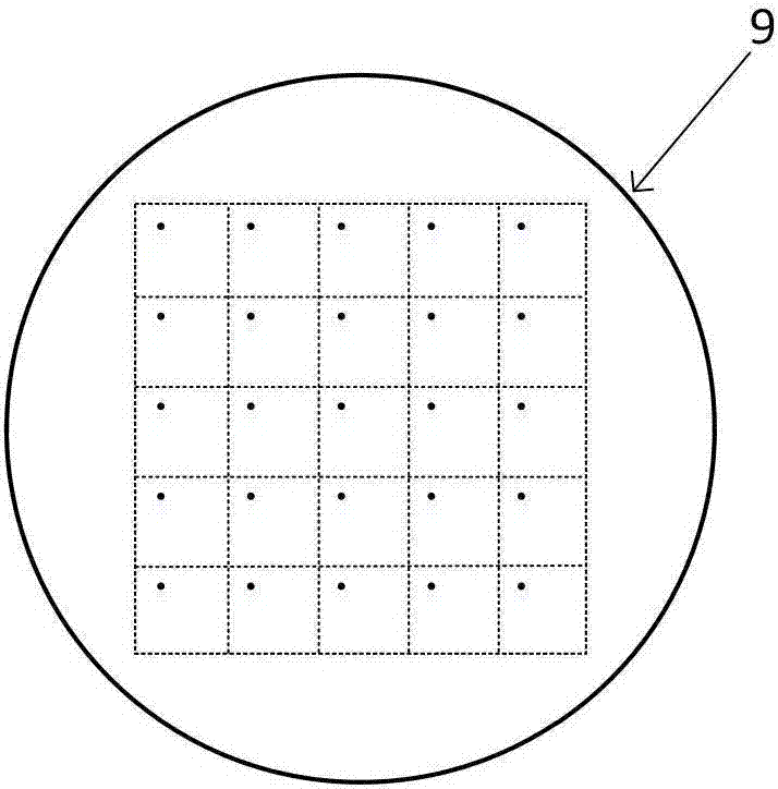
[0030] Such as figure 1 As shown, an ultrafast laser optical chip array processing system of the present invention includes a laser light source 1, a spatial light modulator 2, a beam expander 3, a mirror 4, a microlens array 5, and a six-dimensional working platform along the direction of the optical path 6. In addition, it also includes an air flotation platform 7, a central control computer 8, a base 9, and a vacuum adsorption hole 10;

[0031] The central control computer 8 is respectively connected with the laser light source 1, the spatial light modulator 2, and the six-dimensional working platform 6 for the control of the entire system;

[0032] The air floating platform 7 is arranged under the six-dimensional working platform 6 for carrying the six-dimensional working platfo...


PUM


Abstract

The invention discloses an ultrafast-laser optical chip array processing system and method, and belongs to the technical field of micro-nano processing of optical chips. The system comprises a laser light source, a spatial light modulator, a beam expander, a reflector, a micro-lens array and a six-dimensional working platform, and the system further comprises an air-floating platform and a central-control computer, wherein the central-control computer is connected with the laser light source, the spatial light modulator and the six-dimensional working platform and used for control of the whole system, and the air-floating platform is arranged under the six-dimensional working platform and used for bearing the six-dimensional working platform. According to the ultrafast-laser optical chip array processing system and method, a laser array processing method is adopted, dozens of optical chips can be obtained in one-time processing process, the processing efficiency is high, and quality consistency is good; in addition, the laser processing method is adopted, processing equipment is simple, the requirement on the processing environment is low, and therefore the production cost is greatly reduced.

Description

technical field [0001] The invention relates to the technical field of optical chip micro-nano processing, in particular to an ultrafast laser optical chip array processing system and method. Background technique [0002] With the continuous development of optical fiber communication technology, the direction of optical communication broadband construction is gradually shifting from backbone network, metropolitan area network, local area network, etc. to FTTH. As the basic components of FTTH, such as PLC, PLC optical splitter, WDM, AWG, semiconductor laser, grating, etc., are also facing pressure to reduce power consumption and reduce manufacturing costs. [0003] At present, the processing of optical chips has problems such as complex processing procedures, high processing difficulty, and low processing efficiency. Traditional processing methods such as chemical etching and mechanical processing have high requirements for operators. The processing quality and its dependence...

Claims


Application Information

Patent Timeline
Patent Type & Authority Applications(China)
IPC IPC(8): B23K26/362B23K26/067B23K26/064B23K26/70
CPCB23K26/0643B23K26/0648B23K26/0676B23K26/361B23K26/702
Inventor 陶青王珏刘顿陈列娄德元杨奇彪彼得·贝内特翟中生郑重
Owner HUBEI UNIV OF TECH
Why Eureka
Try Eureka