Plasm restraint device

A plasma and confinement device technology, applied in the field of substrate devices, can solve problems such as processing chamber pollution, achieve the effects of preventing pollution, improving utilization, and preventing secondary discharge

Active Publication Date: 2008-03-26
ADVANCED MICRO FAB EQUIP INC CHINA
View PDF3 Cites 20 Cited by
  • Summary
  • Abstract
  • Description
  • Claims
  • Application Information

AI Technical Summary

Problems solved by technology

[0007] The purpose of the present invention is to provide a plasma confinement device, which overcomes the deficiencies of the pri

Method used


Image

  • Plasm restraint device
  • Plasm restraint device
  • Plasm restraint device

Examples


Embodiment approach

[0051] As another embodiment of the present invention, the conductive element 100 may also be formed of a conductive semiconductor material doped with impurities, wherein the impurities are various elements or various elements that can make the semiconductor material conductive In combination, preferably, in this embodiment, the conductive element 100 is formed of a silicon semiconductor material doped with boron or nitrogen.

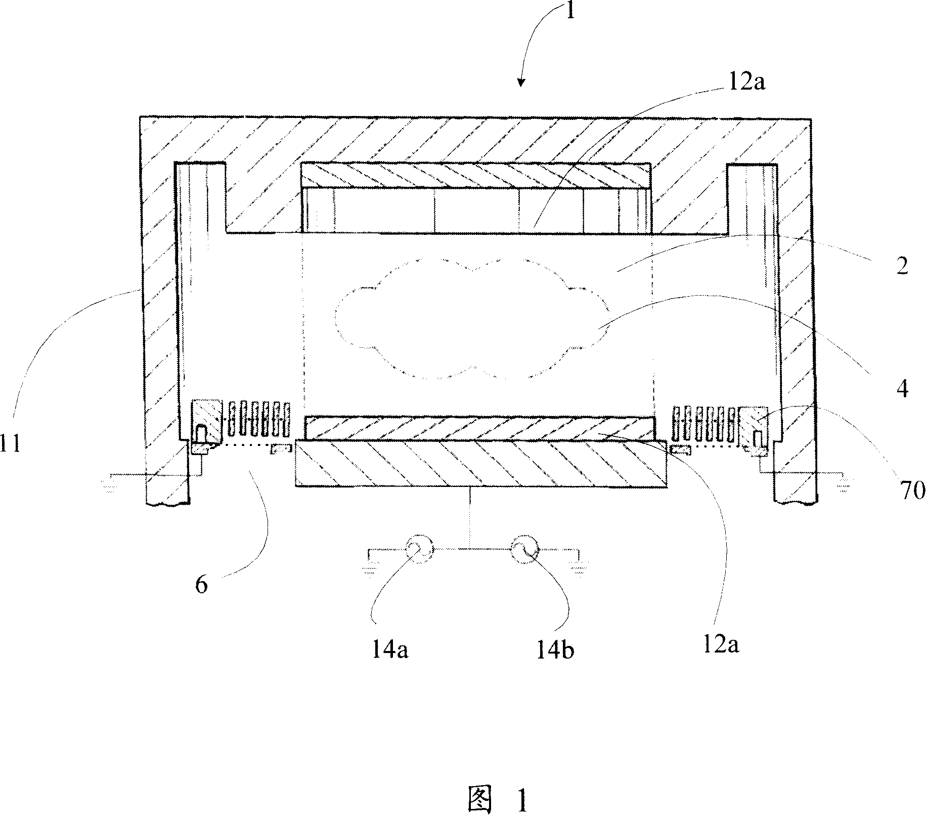
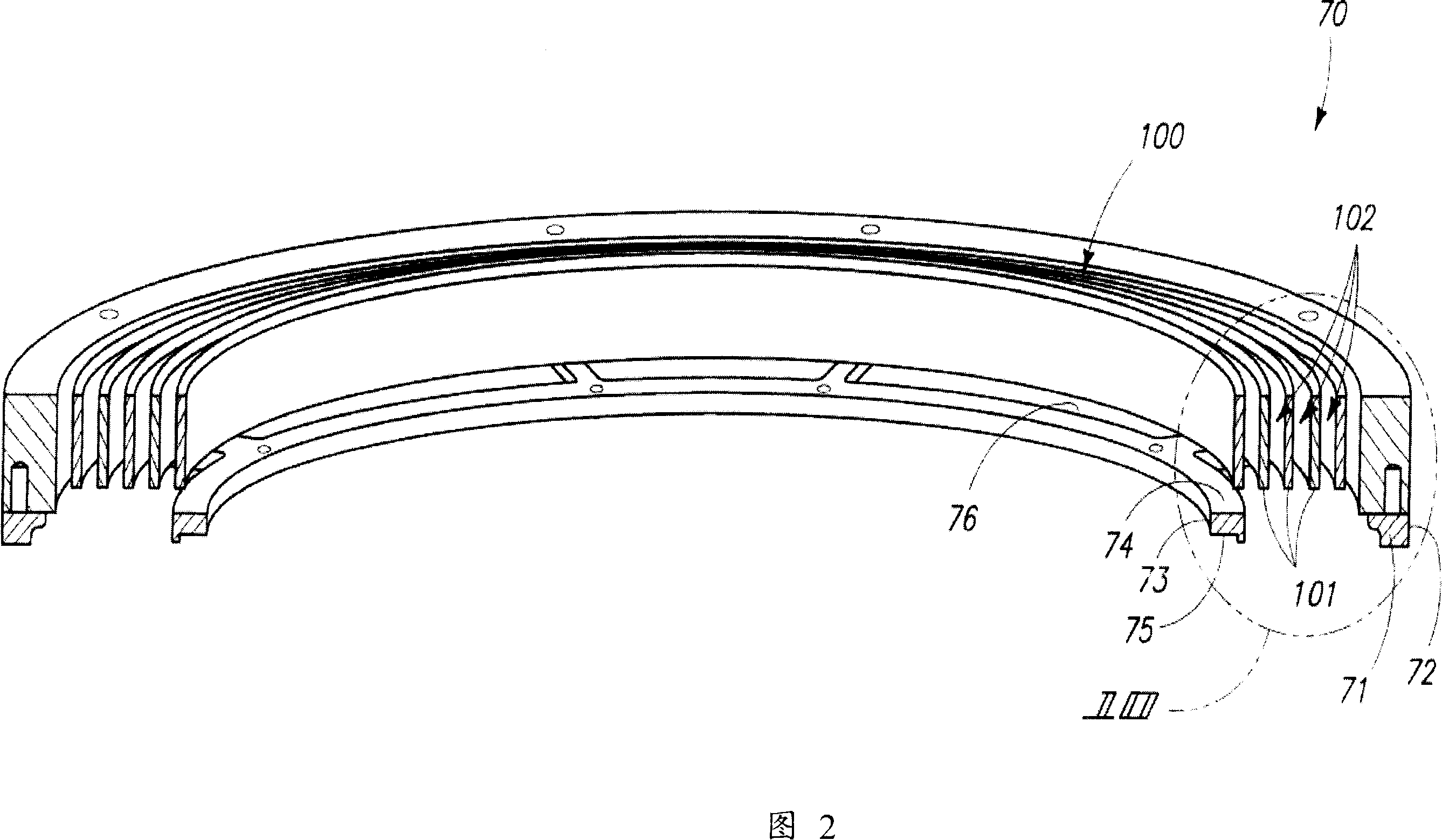
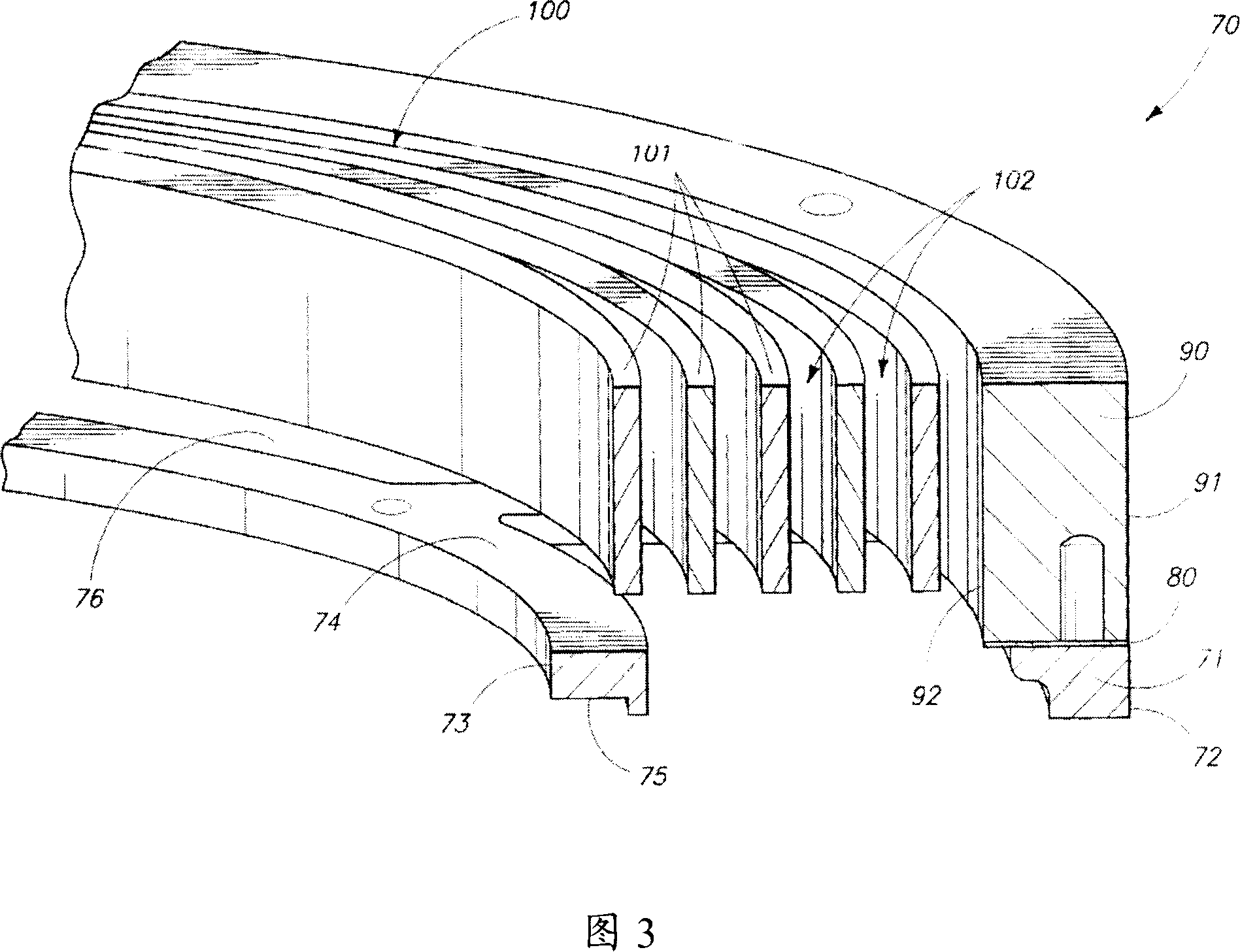
[0052] In the embodiment shown in FIG. 2 and FIG. 3 , the conductive element 100 is formed by a plurality of conductive concentric rings 101 and a conductive support ring 90 , and channels 102 are formed between the conductive concentric rings 101 . As a modification of this embodiment, the conductive element 100 can be an integrally formed conductive plate (not shown), which is arranged around the lower electrode in a substantially ring shape, and is arranged in the processing area and the plasma processing apparatus. Between the exhaust areas, through...


PUM


Abstract

A plasma confinement device used to plasma treatment device is arranged between the treatment zone and the exhaust zone thereof. The plasma confinement device includes an electric element, the electric element is provided with a plurality of channels which are used for controlling the output of used reaction gas and byproduct gas, and electric counteracting electrification particles which pass through the channels, the plasma discharge is basically confined in the treatment zone. The treatment device also includes electric earthing elements are arranged under the electric elements and are insulated from the electric elements. The plasma confinement device of the invention reduces the unhoped plasma which is formed out of the plasma treatment zone thereof, the pollution of the plasma treatment device cavity is solved.

Description

【Technical field】 [0001] The invention relates to a device for processing semiconductor substrates for integrated circuits or for processing glass flat substrates for flat panel displays, in particular to a plasma confinement device in a plasma processing device and related plasma bound method. 【Background technique】 [0002] The plasma processing device uses the working principle of the vacuum reaction chamber to process the semiconductor substrate and the substrate of the plasma flat panel. The working principle of the vacuum reaction chamber is to pass a reaction gas containing an appropriate etchant or deposition source gas into the vacuum reaction chamber, and then input radio frequency energy to the vacuum reaction chamber to activate the reaction gas to ignite and maintain the plasma body, in order to respectively etch the material layer on the surface of the substrate or deposit the material layer on the surface of the substrate, and then process the semiconductor s...

Claims


Application Information

Patent Timeline
IPC IPC(8): H05H1/03H01J37/32H01L21/00
Inventor 倪图强陈金元钱青付越虹徐朝阳周旭升王晔
Owner ADVANCED MICRO FAB EQUIP INC CHINA
Why Eureka
Try Eureka