High resolved micro-three-dimensional image forming apparatus

A three-dimensional imaging, high-resolution technology, used in microscopes, measuring devices, analysis materials, etc., can solve problems such as unrealized, achieve the effect of improving resolution, saving experimental costs and processing cycles, and improving lighting efficiency

Active Publication Date: 2008-05-14
INST OF OPTICS & ELECTRONICS - CHINESE ACAD OF SCI
View PDF0 Cites 9 Cited by
  • Summary
  • Abstract
  • Description
  • Claims
  • Application Information

AI Technical Summary

Problems solved by technology

The far-field super-resolution imaging technology adds a device to the traditional optical imaging system, the so-called metalens device, which can amplify the evanescent wave carrying the high-frequency information of the object and convert it into a propagating wave that can be observed in the far field. Realize high-resolution imaging of objects in the far field. This method is possible for imaging three-dimensional objects, but it has not yet been realized

Method used


Image

  • High resolved micro-three-dimensional image forming apparatus
  • High resolved micro-three-dimensional image forming apparatus
  • High resolved micro-three-dimensional image forming apparatus

Examples


Embodiment Construction

[0037] The present invention will be described in detail below in conjunction with specific implementation methods and accompanying drawings, but the scope of protection of the present invention is not limited to the following examples, but should include all content in the claims.

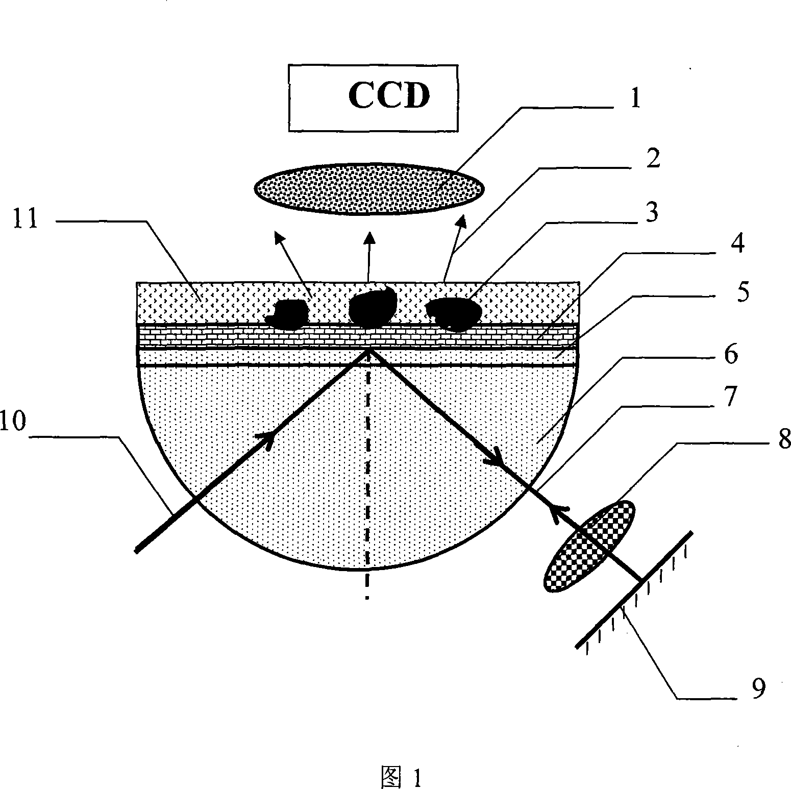
[0038] (1) The wavelength of the incident light is selected as λ=632.8nm, the incident light has not undergone polarization processing and contains TM wave and TE wave;

[0039] (2) The material of the hemispherical prism is K9 glass, and the radius is 20mm;

[0040] (3) select slide glass material to be K9 glass, its thickness is 1mm, adopts the gold of vacuum evaporation 10nm on its surface;

[0041] (4) The glass slide plated with metal gold is placed on the hemispherical plane of the hemispherical prism, and the object is placed on the metal surface on the glass slide. The object is a chromium line with a line width of 160nm and a period of 224nm;

[0042] (5) The incident light is incident o...


PUM

PropertyMeasurementUnit
radiusaaaaaaaaaa
thicknessaaaaaaaaaa
thicknessaaaaaaaaaa

Abstract

A high-resolution microscopic three-dimensional imaging device is characterized by the following steps: first determine the incident light, then select a suitable hemispherical prism, select a slide glass and vapor-deposit a layer of metal on its surface, and place it on the hemispherical plane of the hemispherical prism , put the object on the metal layer, let the incident light be incident on a point on the prism hemispherical surface along the radial direction of the prism, the angle between the incident light and the plane of the glass slide is θ, and the light beam will produce total reflection on the surface of the slide, TM The wave generates surface plasma waves on the metal surface through total reflection, and the TE wave is reflected. A λ/4 wave plate and a mirror are placed on the reflected light path outside the hemispherical prism; the detector is placed above the object to detect and record Detection results; by changing the incident surface and the included angle θ, illuminating the object at different positions and recording the detection results, and considering all the detection results comprehensively, the complete three-dimensional information of the detected object can be obtained; this method can effectively use the lighting light, the device is flexible, and the imaging resolution is high.

Description

technical field [0001] The invention relates to a microscopic imaging device, in particular to a high-resolution microscopic three-dimensional imaging device. Background technique [0002] In recent years, with the rapid development of micro-nano processing technology and nanomaterials, the electromagnetic properties of micro-nano metal structures are receiving more and more attention. The interaction of light with surface micro-nano metal structures produces a series of new and exotic physical phenomena. For example, in 1998, French scientist Ebbesen and his collaborators discovered the phenomenon of extraordinary enhancement (Extraordinary Optical Transmission) of light passing through a subwavelength metal hole array. The research of H.J.Lezec et al. further showed that: when the light passes through the sub-wavelength metal nanohole, its transmittance can not only be enhanced, but also the diffraction angle of the beam is very small, and the transmission direction does ...

Claims


Application Information

Patent Timeline
Patent Type & Authority Applications(China)
IPC IPC(8): G02B21/36G02B21/00G01N21/00
Inventor 罗先刚杨学峰杜春雷史立芳
Owner INST OF OPTICS & ELECTRONICS - CHINESE ACAD OF SCI
Why Eureka
Try Eureka