Scheduling method in silicon chip working process

A technology of processing process and scheduling method, applied in the direction of total factory control, total factory control, electrical program control, etc., can solve the problems of low chamber utilization rate, low production efficiency, long average processing time, etc., and achieve chamber utilization rate High efficiency, high production efficiency, and short average processing time

Active Publication Date: 2008-05-14
BEIJING NAURA MICROELECTRONICS EQUIP CO LTD
View PDF0 Cites 32 Cited by
  • Summary
  • Abstract
  • Description
  • Claims
  • Application Information

AI Technical Summary

Problems solved by technology

In this way, there are situations where the chamber is empty, the utilization rate of the chamber

Method used


Image

  • Scheduling method in silicon chip working process
  • Scheduling method in silicon chip working process
  • Scheduling method in silicon chip working process

Examples


Embodiment Construction

[0038] The scheduling method in the silicon wafer processing process of the present invention is used to schedule the sequence of multiple processing procedures of multiple silicon wafers in the silicon wafer processing equipment, and can also be used to schedule the processing procedures of other equipment.

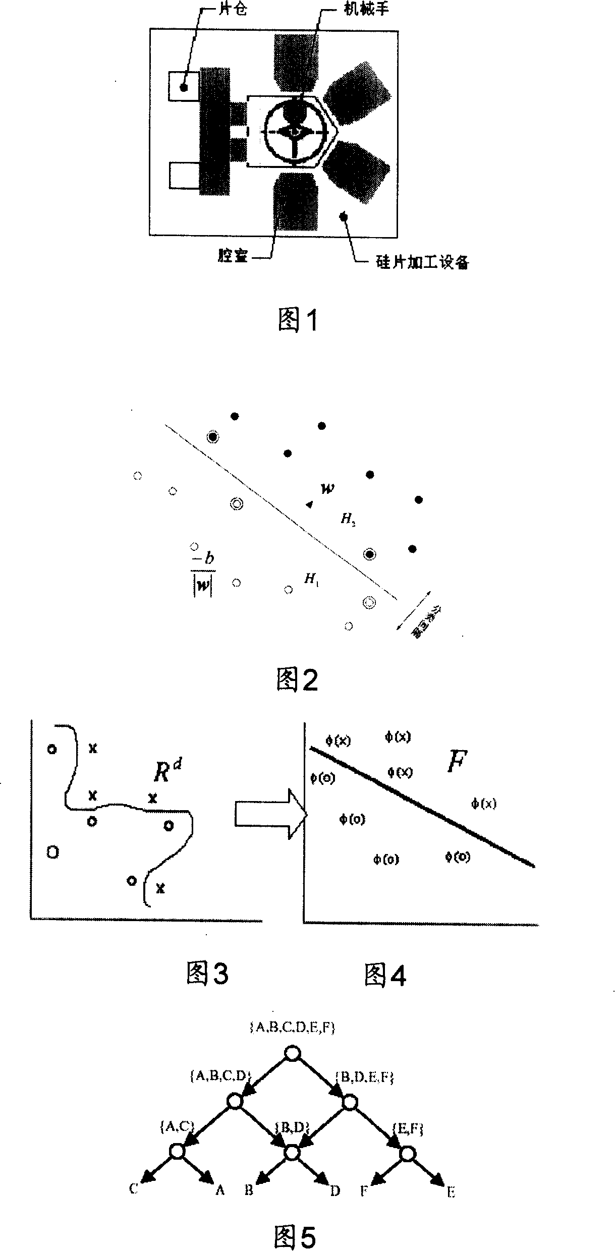
[0039] As shown in Figure 1, the silicon wafer processing equipment includes a magazine, a transfer device and a plurality of chambers, the silicon wafers are processed in the chamber, and the transfer device includes a manipulator for transferring between the magazine and the chamber. Silicon wafers are transported between multiple chambers and among multiple chambers, and the wafer warehouse is used to store silicon wafers in process tasks.

[0040] Its preferred specific implementation method is to schedule in units of procedures. The procedures refer to the processing steps of any silicon wafer in any chamber in a process task. First, multiple procedures are carried o...


PUM


Abstract

The invention discloses a scheduling method in wafer fabrication which is used for scheduling operation sequence of a plurality of processing procedures of processing equipment of a plurality of silicon wafers. The method takes the processing procedure as a unit for scheduling. The processing procedure refers to a processing step of any silicon wafer in any chamber flow field in a process task: firstly, performing queue sequencing of a plurality of processing procedures according to utilization situation of the chamber flow field, then performing downstream processing in turn according to the queue. When performing the queue sequencing, applying multi-class support vector machine to sort according to the chamber flow field preparation time, switch time, idle time after performance of process and relative emergency degree of every working procedure. The utilization rate of chamber flow field is high, the average processing time is short and production efficiency is high. The scheduling method is mainly applicable to the processing procedures of silicon wafer processing equipment and can also be applied to mobilize processing operations of other equipment.

Description

technical field [0001] The invention relates to a production process scheduling method, in particular to a scheduling method in the process of semiconductor silicon chip processing. Background technique [0002] Processing semiconductor silicon wafers requires multiple procedures. The silicon wafer processing equipment includes multiple chambers for processing silicon wafers, such as the reaction chamber for etching silicon wafers; it also includes one or two Loadports. ), which is used to store silicon wafers in process tasks; it also includes a transfer chamber, which is equipped with a single-arm ROBOT (manipulator), which is used to realize the transfer of silicon wafers from the Loadport to the chamber and between different chambers. transfer between rooms. Each process task contains a Cassette (silicon wafer box), and the Cassette is placed in the Loadport. There are at most 25 silicon wafers in each Cassette, and at least 1 silicon wafer. Each silicon wafer goes thr...

Claims


Application Information

Patent Timeline
IPC IPC(8): H01L21/677H01L21/00G05B19/418
CPCY02P90/02
Inventor 崔琳
Owner BEIJING NAURA MICROELECTRONICS EQUIP CO LTD
Why Eureka
Try Eureka