Optical tool and method for forming soldering-resistant pattern

A pattern and solder mask technology, applied in the field of exposure processing, which can solve problems such as the diameter of the through hole being smaller than the design value, the vignetting on the surface, and the width of the line.

Active Publication Date: 2008-05-21
TAIYO INK MFG CO LTD
View PDF7 Cites 7 Cited by
  • Summary
  • Abstract
  • Description
  • Claims
  • Application Information

AI Technical Summary

Problems solved by technology

However, in this countermeasure, there are many inappropriate problems such as vignetting on the surface layer, line width becoming wider than the design value, and via hole diameter becoming smaller than the design value.
On the other hand, if the exposure amount is low as it is, a sufficient curing depth cannot be obtained, and there is a problem of undercutting.

Method used


Image

  • Optical tool and method for forming soldering-resistant pattern
  • Optical tool and method for forming soldering-resistant pattern
  • Optical tool and method for forming soldering-resistant pattern

Examples


Embodiment

[0123] Hereinafter, although an Example and a comparative example are shown and this invention is concretely demonstrated, it is needless to say that this invention is not limited to a following example.

Synthetic example 1

[0125] Add 660 g of cresol novolak type epoxy resin (manufactured by Nippon Kayaku Co., Ltd., EOCN-104S, soften Point 92°C, epoxy equivalent = 220g / equivalent), 421.3g carbitol acetate and 180.6g solvent naphtha, heated to 90°C and stirred to dissolve. Then, it was cooled to 60° C., 216 g of acrylic acid, 4.0 g of triphenylphosphine, and 1.3 g of methylhydroquinone were added, and reacted at 100° C. for 12 hours to obtain a reaction product having an acid value of 0.2 mgKOH / g. 241.7 g of tetrahydrophthalic anhydride was added thereto, heated to 90° C., and reacted for 6 hours. Thus, the content of non-volatile matter = 65% by mass, solid content acid value = 77 mgKOH / g, double bond equivalent (g weight of resin per 1 mole of unsaturated group) = 400 g / equivalent, and weight average molecular weight = 7000 was obtained. A solution of a carboxylic acid photosensitive resin (A). Hereinafter, the solution of this carboxylic acid-containing photosensitive resin is called varnish ...

Embodiment 1

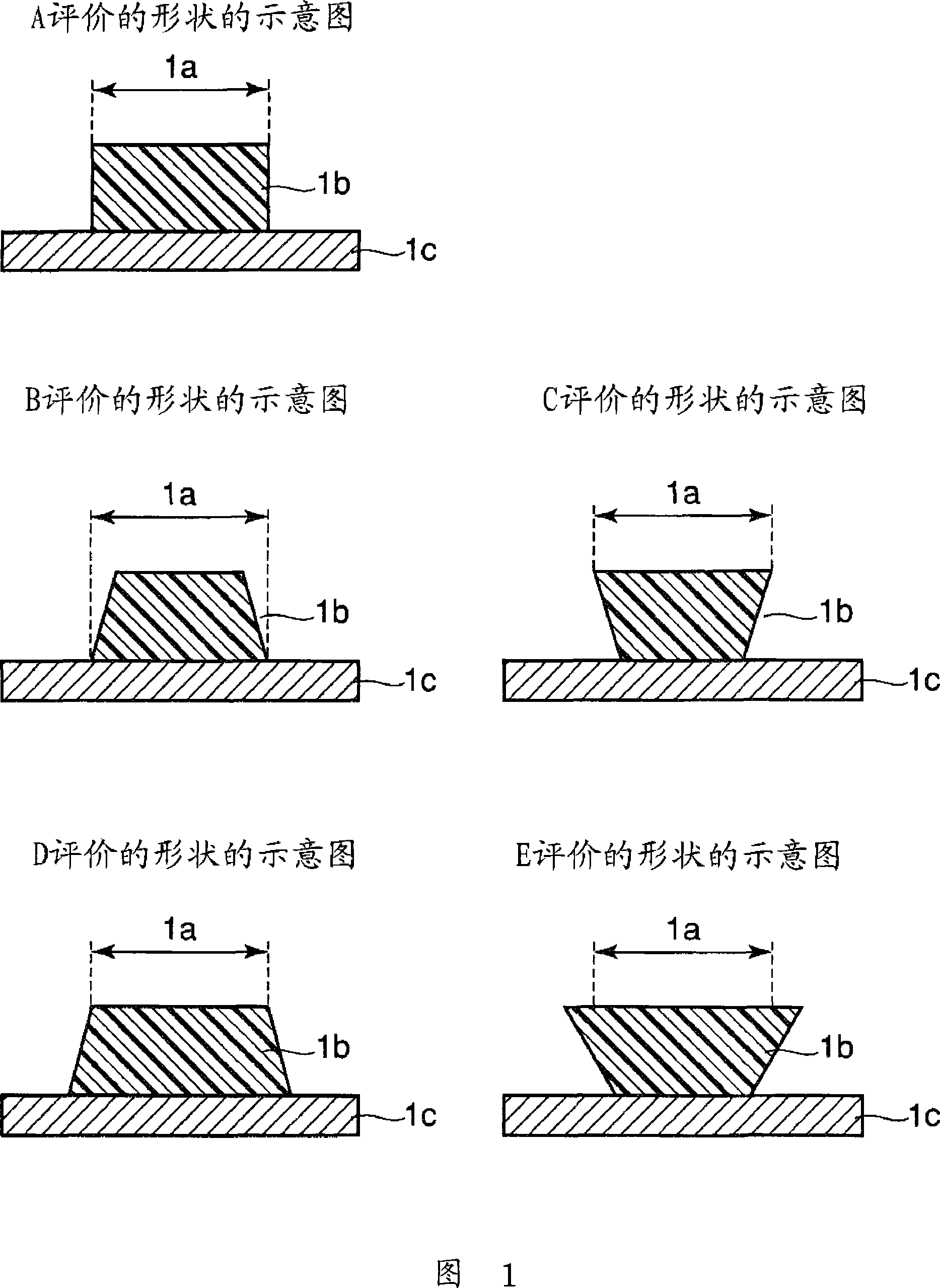
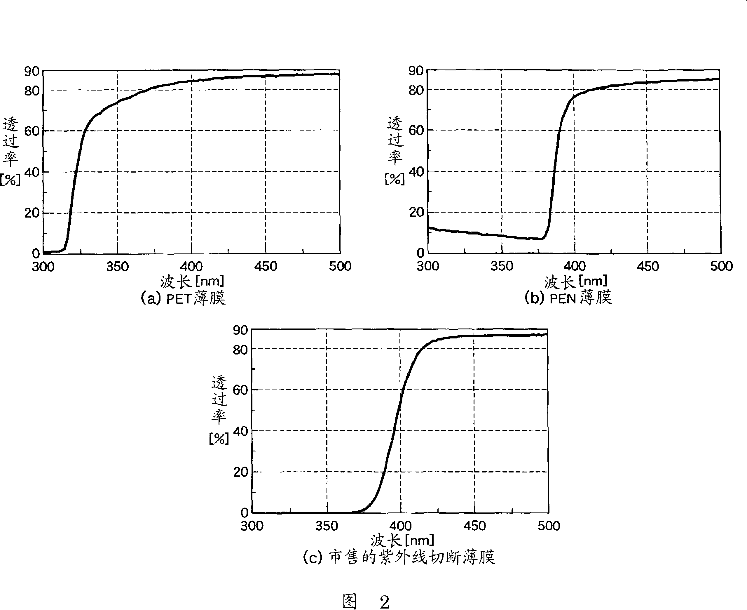
[0153] (Example 1: Using a PEN-based film as a protective film / resist film thickness 18 μm)

[0154] The same test as in Comparative Example 1 was performed except that a polyethylene naphthalate film was used instead of the polyethylene terephthalate film as the protective film. The evaluation results of the cross-sectional shapes of the obtained solder resist patterns are the same as those in Table 3. In addition, the photomask was in a clean state with no defects and no resist adhesion.


PUM

PropertyMeasurementUnit
thicknessaaaaaaaaaa
acid valueaaaaaaaaaa

Abstract

The invention provides an exposure processing technique for a solder mask, which can form a corrosion resistance pattern with good reproducibility and high resolution without being influenced by the thickness of the solder mask and the blue paints. The invention provides an exposure processing technique for a solder mask during the pattern forming process, wherein, a film or an optical tool having the film is used for cutting 50% of lights below 370nm and permeating 80% of lights above 400nm.

Description

technical field [0001] The present invention relates to exposure processing technology when forming solder resist patterns of printed circuit boards. Background technique [0002] Generally, a printed circuit board is formed with a solder resist layer on its outermost layer. This solder resist layer is formed through the steps of coating a photosensitive composition on a base material on which a wiring circuit is formed, inserting a photomask to selectively expose the obtained coating film, and developing the unexposed part. A pattern is formed and then thermally cured by heating. [0003] In forming such a solder resist layer, a polyethylene terephthalate (PET) film or glass is used as a material for a photomask. Wherein, PET film is cheap and has flexibility, can make the light of more than 300nm ultraviolet region pass through more than 90% and can irradiate sufficient amount of ultraviolet light to photosensitive composition, therefore, be widely used as photomask (for...

Claims


Application Information

Patent Timeline
Patent Type & Authority Applications(China)
IPC IPC(8): G03F1/00G03F7/004G03F7/00H05K3/00G03F1/48G03F1/54G03F1/56G03F7/029G03F7/031G03F7/20H05K3/28
Inventor 柴崎阳子加藤贤治有马圣夫
Owner TAIYO INK MFG CO LTD
Why Eureka
Try Eureka