Method for analyzing and increasing yield of semi-conductor production line

A yield and production line technology, applied in the field of analyzing and improving the yield of integrated circuits, can solve the problems of different sensitivities, low efficiency of measuring equipment, and increase the difficulty of setting effective sensitivity, so as to achieve the effect of improving the speed of improvement.

Active Publication Date: 2008-05-21
SEMITRONIX
View PDF0 Cites 21 Cited by
  • Summary
  • Abstract
  • Description
  • Claims
  • Application Information

AI Technical Summary

Problems solved by technology

From the above process, it can be seen that this assignment is more of an accumulation of experience, and there is no specific quantitative method, so it is impossible to accurately calculate the impact of each layer and a process module defect on the yield
[0006] 2) This yield model only considers the area of ​​the entire chip, and does not take into account the difference in layout design parameters
However, this setting is mostly based on experience, and it cannot be theoretically set accurately so that the equipment can detect all or most of the defects.
In addition, the sensitivity ...

Method used


Image

  • Method for analyzing and increasing yield of semi-conductor production line
  • Method for analyzing and increasing yield of semi-conductor production line
  • Method for analyzing and increasing yield of semi-conductor production line

Examples


Embodiment Construction

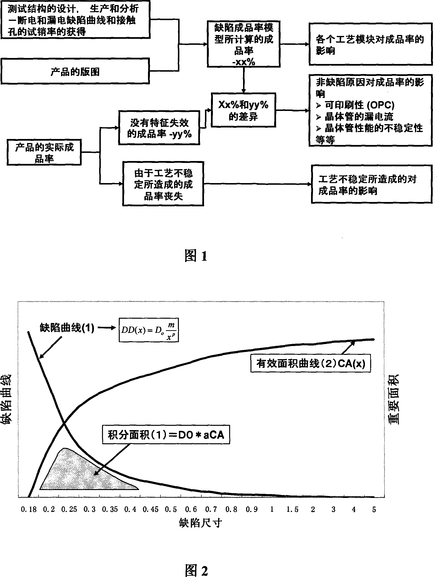
[0118] Now adopt typical data to illustrate the present invention in conjunction with the program flow of Fig. 1:

[0119] 1. Acquisition of defect curves of various process modules in semiconductor production lines

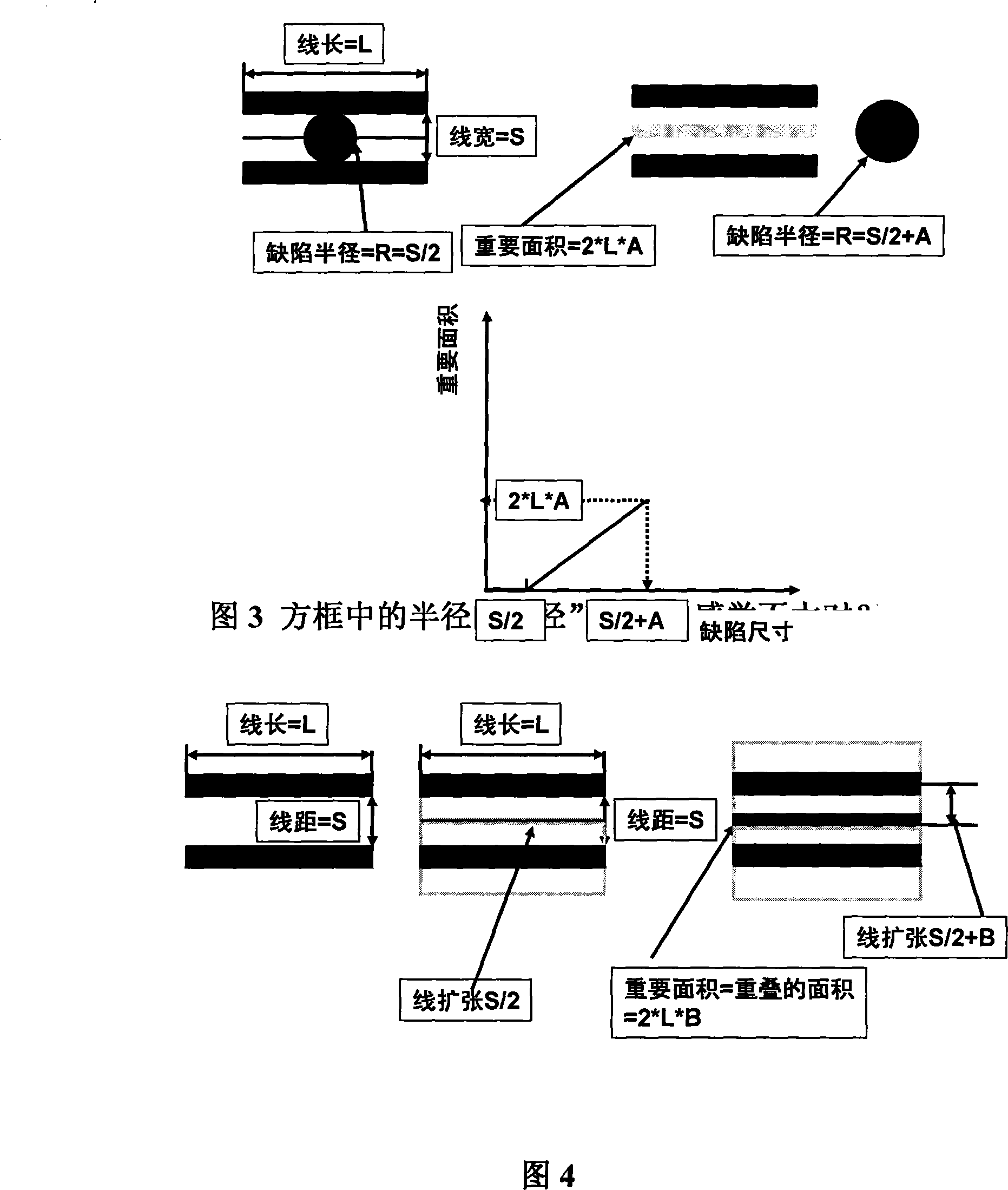
[0120] FIG. 7 shows a test circuit in a test chip for obtaining the defect rate of the first-layer metal M1 of power-off and leakage. This is a collection of comb-shaped and P snake-shaped metal wires.

[0121] Here, P=4 is used to illustrate how to obtain the defect rate curves of power failure and leakage through electrical measurement.

[0122] For the power down measurement, there will be 4 measurements - Line 1, Line 2, Line 3 and Line 4.

[0123] For leakage measurement, there will be 3 measurements - leakage from line 1 to line 2, leakage from line 2 to line 3, and leakage from line 3 to line 4.

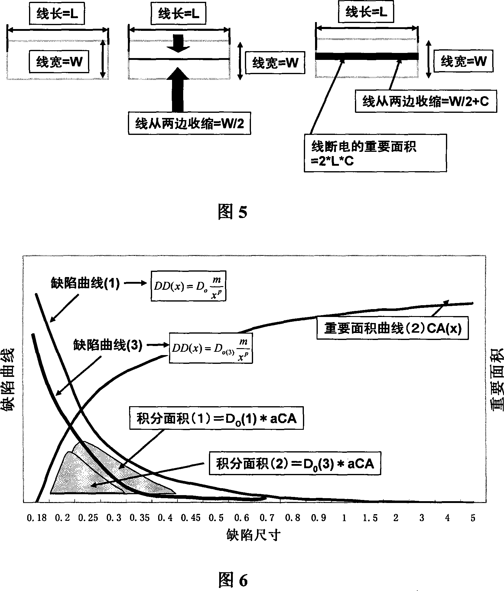
[0124] For the measurement of power failure, in a tested circuit unit, the following situations will occur:

[0125] 1) A single line is broken (no adjacent ...


PUM


Abstract

The invention discloses a method used for analyzing and improving yield of semiconductor production line. The invention is characterized in that a test chip is used for precisely determining the defect rate curves of various process modules of the production line and the failure rate of contact holes, and an effective area curve of power off, an effective area curve of leakage of each layer of product layout and the number of the contact holes are analyzed, and a model framework of the yield then can be built. The invention has the advantages that the invention can precisely calculate different effects of defect rates of various process modules on the yield and the invention enables production personnel to exactly know the effects of various process modules of the production line on the yield, thus the engineering personnel of the production line can be instructed to rapidly and effectively solve the deficiencies seriously affecting the yield, and the yield then can be improved rapidly and effectively.

Description

technical field [0001] The invention belongs to the field of integrated circuit manufacturing, in particular to a method for analyzing and improving the yield of integrated circuits. Background technique [0002] The yield rate of semiconductors and the speed of technology maturity determine whether a semiconductor manufacturer is profitable. How to improve the yield rate better and faster is an urgent problem to be solved. It is very important to establish an effective yield model and be able to quickly reduce fatal defects. Traditionally, the yield model uses the entire area of ​​the chip and the defect rate of each layer or each process module estimated from the optical measurement equipment to estimate the yield. The commonly used BOSE-EINSTEIN model is shown in formula (1). [0003] Y = Y s Π Layer 1 ( 1 + ...

Claims


Application Information

Patent Timeline
IPC IPC(8): G06F17/50H01L21/00H01L21/66G01R31/308
Inventor 马铁中郑勇军史峥严晓浪
Owner SEMITRONIX
Why Eureka
Try Eureka