Display panel and its structure

A display panel and transistor technology, applied to static indicators, instruments, electrical components, etc., can solve the problems of increased power consumption, increased wiring difficulty, and low aperture ratio of the display panel, achieving the goal of increasing aperture ratio and reducing power The effect of consumption

Active Publication Date: 2008-06-04
INNOLUX CORP +1
View PDF1 Cites 17 Cited by
  • Summary
  • Abstract
  • Description
  • Claims
  • Application Information

AI Technical Summary

Problems solved by technology

[0006] 1. Since there are four transistors in one pixel, it will increase the difficulty of wiring (Layout), and the power consumption will also increase accordingly
[0007] 2. Due to too many components in one pixel, the aperture ratio of the display panel will also be reduced

Method used


Image

  • Display panel and its structure
  • Display panel and its structure
  • Display panel and its structure

Examples


Embodiment Construction

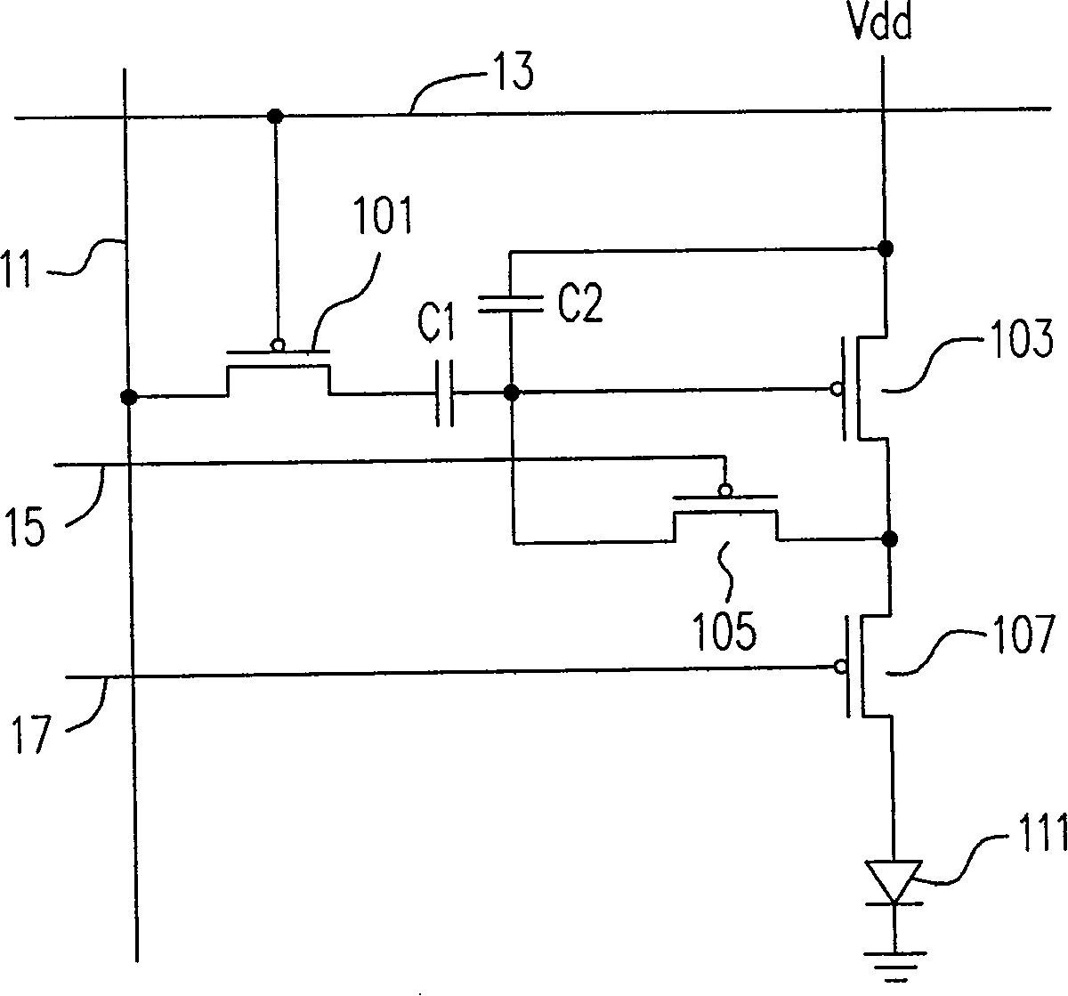
[0050] Preferred embodiments of the present invention will be described in detail below with reference to the accompanying drawings. The drawings attached hereto illustrate various preferred embodiments of the present invention. The types of transistors described below, such as PMOS transistors, are preferred embodiments of the present invention. However, those skilled in the art can replace it with other types of transistors according to actual conditions without affecting the main spirit of the present invention.

[0051] In addition, the voltage value of the anode voltage described in the following paragraphs will be greater than the voltage value of the cathode voltage described in the following paragraphs, and will not be specifically explained in the following paragraphs.

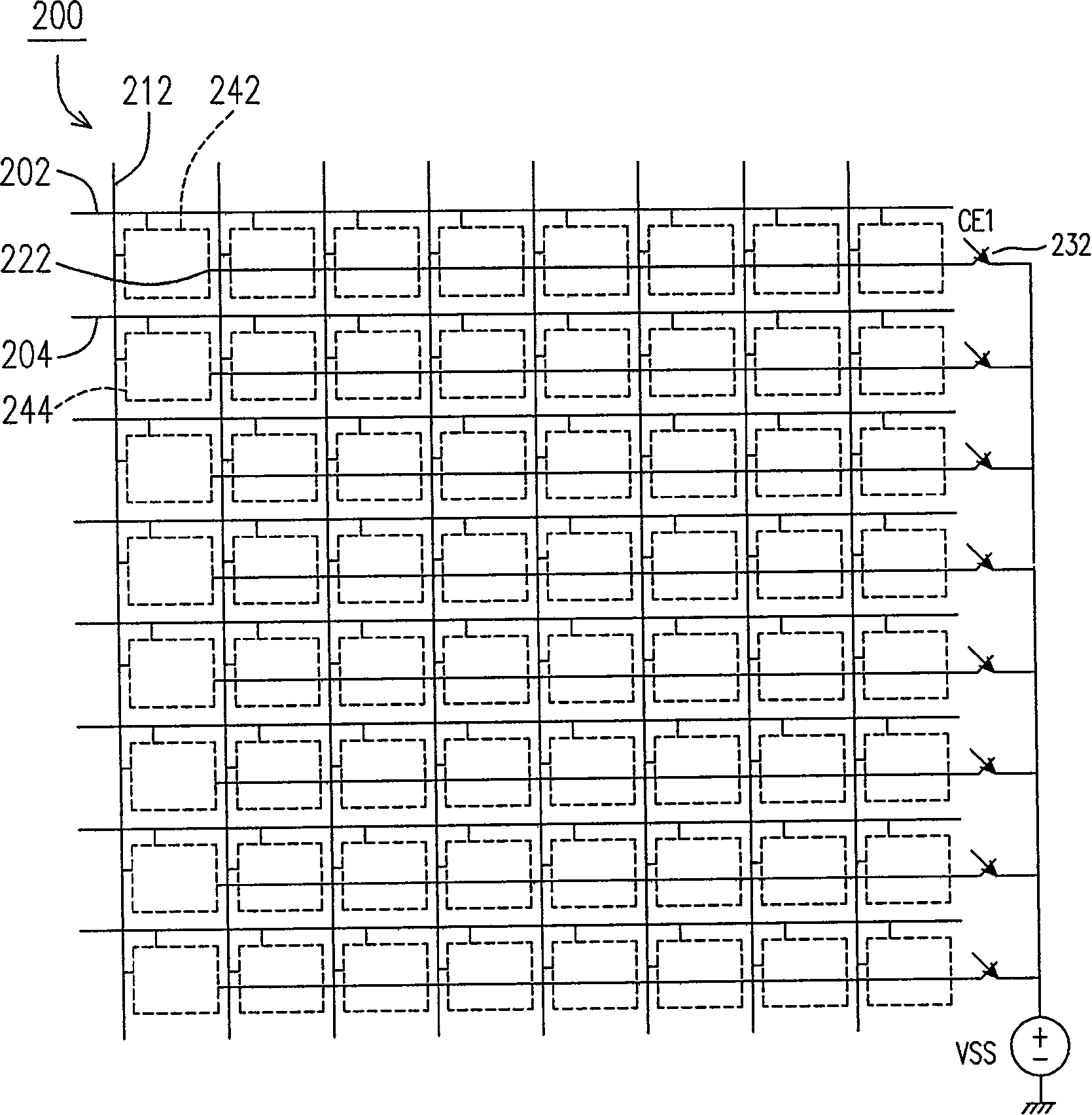
[0052] figure 2 A circuit diagram of a display panel according to a preferred embodiment of the present invention is shown. Please refer to figure 2 , in the display panel 200 provided by the pr...


PUM


Abstract

The invention discloses a display panel and a structure thereof, which comprise a plurality of scanning lines and a plurality of data lines. A pixel circuit is configured at the position where each scanning line is intersected with each data line. In addition, the display panel disclosed by the invention is also provided with a plurality of cathode wires, which are parallel to the scanning lines; among which, all the pixel circuits on the same scanning line are coupled with the same cathode wire and each cathode wire is coupled to a cathode voltage through a switching circuit, and various switching circuits determines whether to conduct the cathode voltage to the corresponding cathode wire according to a control signal. As the elements in the single pixel circuit are reduced, the difficulty of wiring can be lowered, the aperture ratio of the display panel can be increased, the life of the organic light emitting diode element can be extended, and the quality of the picture on the display panel can be kept. The working current in the pixel circuit is stabilized, and the service life of the pixel circuit is extended.

Description

technical field [0001] The present invention relates to a structure of a display panel, and in particular relates to a display panel with common cathode lines and its structure. Background technique [0002] Due to the rapid progress of the multimedia society, the technologies of semiconductor devices and display devices have also made rapid progress. As far as the display is concerned, organic light-emitting displays have no viewing angle limitation, low manufacturing cost, high response speed (about a hundred times higher than that of liquid crystal), power saving, DC drive that can be used in portable machines, wide operating temperature range and weight It is light and can be miniaturized and thinned along with the hardware equipment, etc., which meets the characteristic requirements of the display in the multimedia era. Therefore, organic light-emitting diode displays (OLEDs) have great development potential and are expected to become novel flat-panel displays of the n...

Claims


Application Information

Patent Timeline
Patent Type & Authority Applications(China)
IPC IPC(8): G09G3/32G09G3/30G09G3/20H05B33/08H05B33/14H05B37/02H01L27/32H01L51/50G09G3/3233G09G3/325G09G3/3266H05B44/00
Inventor 郭鸿儒黄建翔曾名骏
Owner INNOLUX CORP
Why Eureka
Try Eureka