Image processing device and method for image sensor

An image processing device and image sensor technology, applied in the field of image processing, can solve the problems of reducing image signal-to-noise ratio, affecting image quality, and high hardware overhead, and achieve the effects of improving signal-to-noise ratio, eliminating noise, and improving quality

Inactive Publication Date: 2008-06-04
BEIJING SUPERPIX MICRO TECHNOLOGY CO LTD
View PDF0 Cites 31 Cited by
  • Summary
  • Abstract
  • Description
  • Claims
  • Application Information

AI Technical Summary

Problems solved by technology

[0010] The disadvantage of the image processing device of the above-mentioned prior art is that it is necessary to perform a gamma transformation on each of the three channels of red, green and blue. resulting in high hardware overhead
Multiple gamma transformations will also introduce more noise, which reduces the signal-to-noise ratio of the image and affects the quality of the image

Method used


Image

  • Image processing device and method for image sensor
  • Image processing device and method for image sensor
  • Image processing device and method for image sensor

Examples


Embodiment Construction

[0028] The invention provides an image processing device and method of an image sensor.

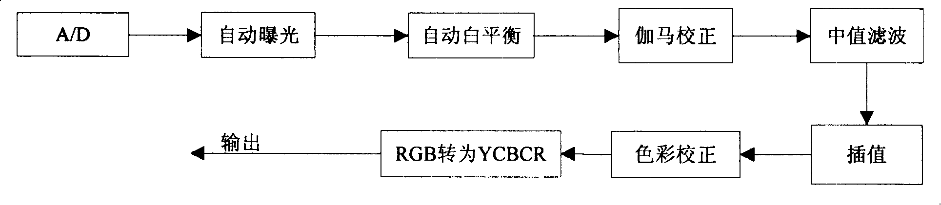
[0029] Describe the present invention in detail below in conjunction with accompanying drawing, the structure of the embodiment of device of the present invention is as follows image 3 As shown, it includes: A / D module, automatic exposure module, automatic white balance module, gamma correction module, interpolation module, color correction module and color space conversion module (RGB to YCBCR module).

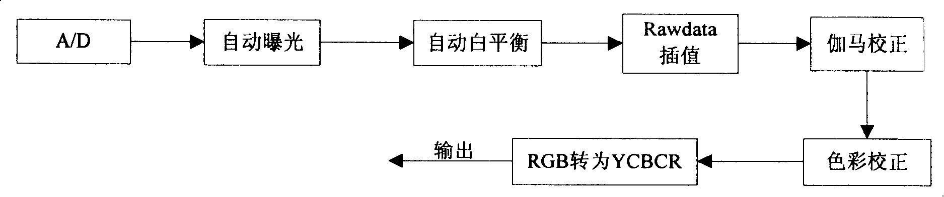
[0030] The device of the present invention and figure 1 The main difference of the shown prior art device is that the correction module is placed before the interpolation module, and the gamma correction process is performed on the image data of only one of the three channels of red, green and blue.

[0031] The function of each module in the image processing device of the present invention will be respectively introduced below according to the order of image data from input to output....


PUM


Abstract

The invention provides a device for processing the image of an image sensor and a method thereof. The device mainly includes a gamma correction module, a median filter module and an interpolation module. The method mainly includes the following steps: image data of red, green or blue channels collected by the image sensor is processed by means of nonlinear transforming; according to the magnitude of signal-to-noise ratio of the image data processed by nonlinear transforming, the image data is processed by corresponding median filtering; and the image data of the red, green or blue channels processed by the median filtering is processed by means of interpolatory calculation to obtain the image data of the red, green, blue three channels and the obtained image data is outputted. By using the invention, hardware overhead of the image sensor can be saved and the signal-to-noise ratio of image output of the image sensor can be improved.

Description

technical field [0001] The invention relates to the field of image processing, in particular to an image processing device and method for an image sensor. Background technique [0002] CMOS (complementary metal-oxide semiconductor, complementary metal-oxide semiconductor) image sensor has been widely used due to its small size, low power consumption, low cost and high integration, accounting for a large proportion of low-end market. [0003] The CMOS image sensor chip integrates automatic white balance, automatic exposure control, automatic gain control, automatic brightness control and other functions, which greatly reduces the complexity of the system and reduces the cost. Therefore, CMOS image sensors have become a hot spot in research and development, and are more widely used in video surveillance and multimedia fields with low price, practical image quality and relatively small power consumption. [0004] When converting the actual scene into image data, the best solu...

Claims


Application Information

Patent Timeline
Patent Type & Authority Applications(China)
IPC IPC(8): H04N9/04H04N9/69H04N9/73H04N9/64
Inventor 李治玮王超银江明
Owner BEIJING SUPERPIX MICRO TECHNOLOGY CO LTD
Why Eureka
Try Eureka