Method for controlling plating layer thickness distribution in FPC making process
A technology of manufacturing process and coating thickness, applied in printed circuit manufacturing, printed circuits, electrical components, etc., can solve the problem of uneven thickness distribution of nickel plating layer, and achieve the improvement of nickel layer thickness distribution ability, uniform distribution ability, and improved nickel plating thickness. The effect of the ability to distribute the current evenly
- Summary
- Abstract
- Description
- Claims
- Application Information
AI Technical Summary
Problems solved by technology
Method used
Image
Examples
Embodiment Construction
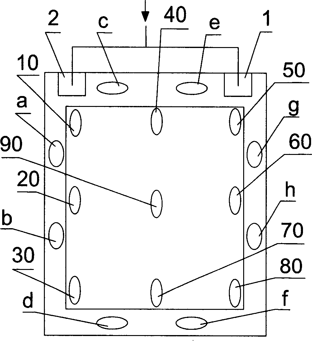
[0015] A kind of method (please refer to figure 1 ), in order to increase the distribution uniformity of the thickness of the nickel plating layer, some openings a, b, c, d, e, f can be added on the outside of the position 10, 20, 30, 40, 50, 60, 70, 80 on the product , g, h (the shape of these openings can be processed into any shape such as circle, ellipse, square, etc. according to the processing conditions), so that the positions 10, 20, 30, 40, 50, 60, 70, and 80 after processing are changed from before to The position around the product is changed to the inside of the product, and the edge effect is added to the positions of openings a, b, c, d, e, f, g, and h, thereby reducing the position 10, 20, 30, 40, 50 , 60, 70, and 80 edge effects, so that the distribution of the thickness of the nickel plating layer can be more uniform.
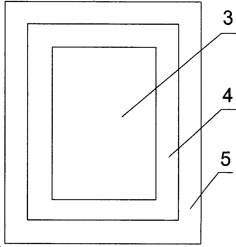
[0016] Increase the opening at the appropriate position, that is to minimize the edge effect, please refer to figure 2 , if the plating sur...
PUM
 Abstract
Description
Claims
Application Information


