Method for forming interlaminar capacitor

A technology for capacitors and capacitor dielectrics, which is applied in the manufacture of circuits, electrical components, semiconductor/solid-state devices, etc., can solve the problems of complex formation processes, and achieve the effect of simplifying the process flow and reducing the number of deposition and etching.

Inactive Publication Date: 2008-06-11
SHANGHAI INTEGRATED CIRCUIT RES & DEV CENT
View PDF0 Cites 2 Cited by
  • Summary
  • Abstract
  • Description
  • Claims
  • Application Information

AI Technical Summary

Problems solved by technology

It can be seen that the formation process of traditional polysilicon and metal interlayer capacitors is complicated, and it needs multiple depositions and etchings to complete.

Method used


Image

  • Method for forming interlaminar capacitor
  • Method for forming interlaminar capacitor
  • Method for forming interlaminar capacitor

Examples


Embodiment Construction

[0030] In order to make the purpose and features of the present invention more comprehensible, the specific implementation manners of the present invention will be further described below in conjunction with the accompanying drawings.

[0031] Please refer to FIG. 2 to FIG. 10 , which are schematic diagrams of the formation process of the interlayer capacitor according to an embodiment of the present invention. details as follows:

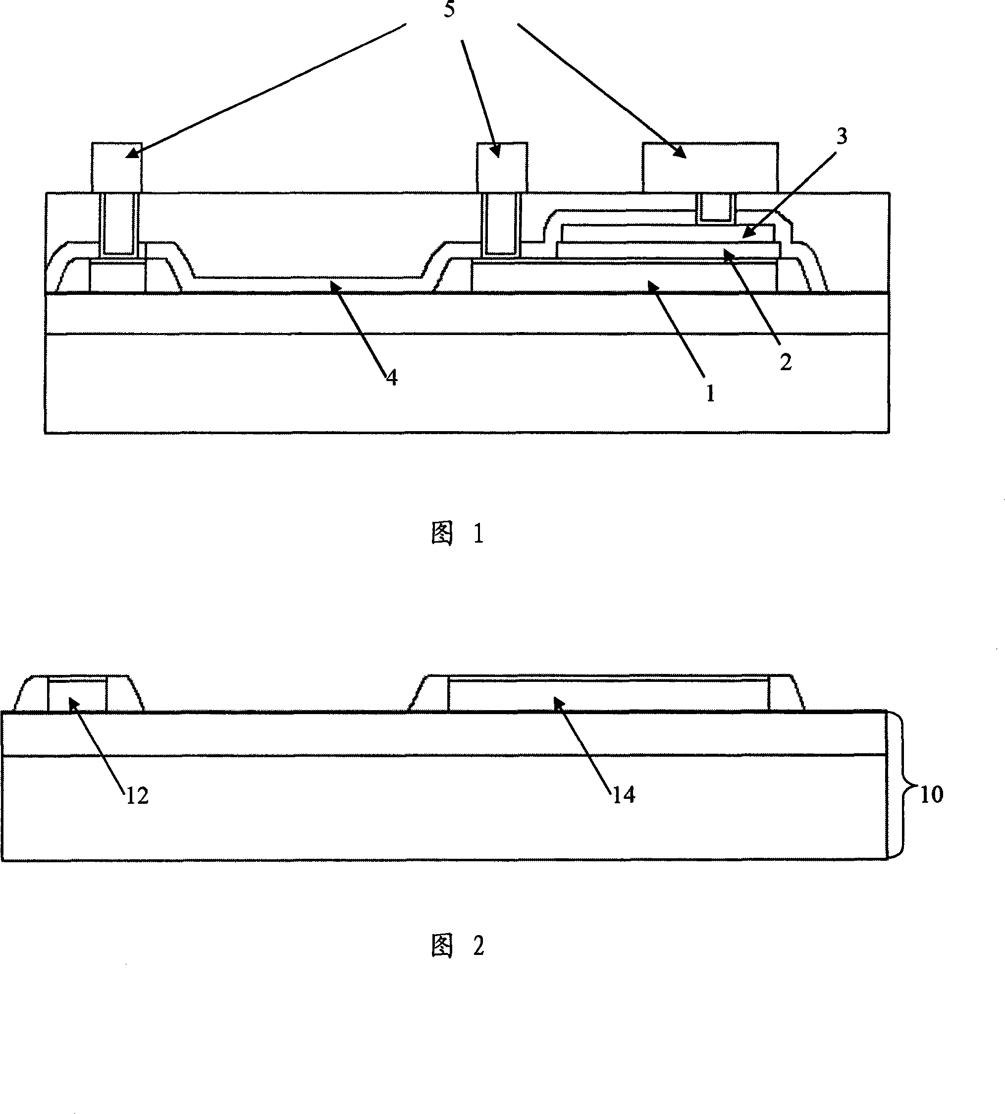
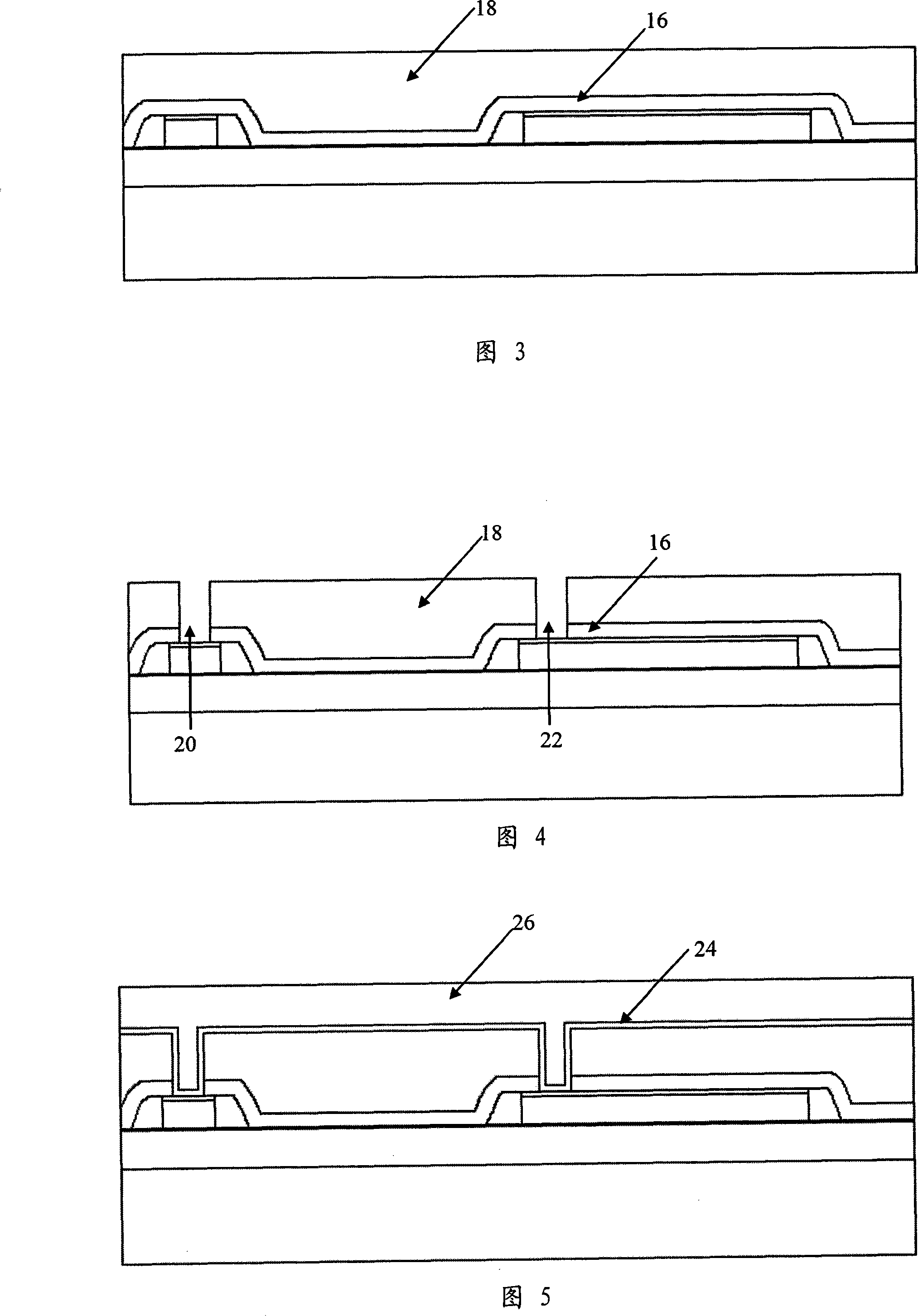
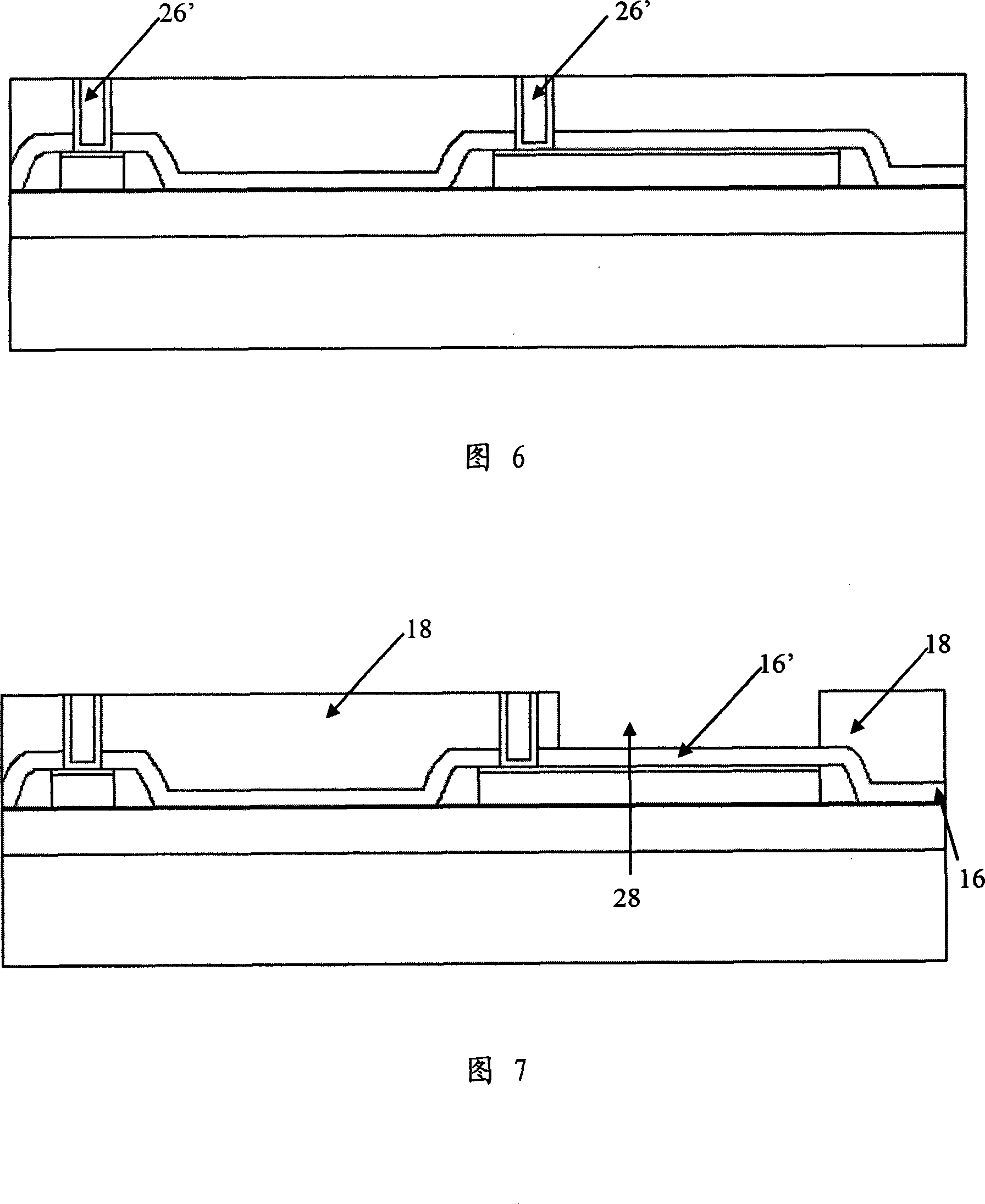
[0032] First, form the gate 12 and the lower plate 14 of the capacitor on the substrate 10 (as shown in FIG. 2); The electrode 12 and the lower plate 14 of the capacitor can then enter the traditional sidewall formation and silicide formation process, forming sidewalls on the side walls of the grid 12 and the lower plate 14 of the capacitor, and forming a silicide layer on the upper surface. Next, an etch stop layer 16 and an interlayer dielectric film 18 are deposited (as shown in FIG. 3 ). Then contact holes 20 and 22 are formed in the interlay...


PUM


Abstract

The invention discloses a forming method of layer capacitor, which uses an etch stop layer as capacitor medium without extra medium layer to deposit and form the capacitor medium, and form an upper metal connecting line and a capacitor upper pole plate by using the same metal layer. The method specifically comprises the following steps of: depositing the etch stop layer and an inter-level dielectrics film after a capacitor lower pole plate is formed; a capacitor plate groove is formed in the inter-level dielectrics firm by etching, wherein, the capacitor plate groove passes the inter-level dielectrics film and stops at the etch stop layer and part of the etch stop layer is exposed, and further the exposed etch stop layer is used as the capacitor medium; and forming the capacitor upper pole plate in the capacitor plate groove. Compared with the prior art, the invention reduces times for depositing and etching and simplifies the process flow.

Description

technical field [0001] The invention relates to an integrated circuit process method, in particular to a method for forming an interlayer capacitor. Background technique [0002] Plate capacitors are widely used in integrated circuits, which include upper and lower layers of conductive materials and a middle dielectric layer. The types of capacitors that are often used include junction capacitance, metal-oxide-silicon capacitance, polycrystalline interlayer capacitance, and metal interlayer capacitance. Due to the large parasitic capacitance and resistance of the first two capacitors, the effective voltage applied to the actually used capacitor is affected. However, polycrystalline interlayer capacitors and metal interlayer capacitors can provide better performance due to the good conductivity of the upper and lower plates. However, the formation process of the polycrystalline interlayer capacitor and the metal interlayer capacitor is complicated, which increases the corre...

Claims


Application Information

Patent Timeline
Patent Type & Authority Applications(China)
IPC IPC(8): H01L21/02H01L21/768
Inventor 顾学强
Owner SHANGHAI INTEGRATED CIRCUIT RES & DEV CENT
Why Eureka
Try Eureka