Supercharge Your Innovation With Domain-Expert AI Agents!

Stackable semiconductor packaging structure

A packaging structure and semiconductor technology, which is applied in the direction of semiconductor devices, semiconductor/solid-state device parts, electric solid-state devices, etc., can solve the problems of area limitation, the overall thickness cannot be effectively reduced, and the second substrate 13 is broken, so as to achieve the goal of reducing the thickness Effect

Active Publication Date: 2008-06-11
ADVANCED SEMICON ENG INC
View PDF0 Cites 2 Cited by
  • Summary
  • Abstract
  • Description
  • Claims
  • Application Information

AI Technical Summary

Problems solved by technology

First of all, since the second substrate 13 has a floating portion, the first pads 133 are located on the periphery of the relative position of the chip 12 (that is, the floating portion), and the relative position of the first bonding pads 133 and the edge of the chip 12 The distance between them is defined as a suspended length L1. Experiments have shown that when the suspended length L1 is more than three times greater than the thickness T1 of the second substrate 13, during wire bonding (Wire Bonding) operations, the suspended part will shake or It is a situation of shock, which is not conducive to the progress of wire-making operations
What's more, when the second substrate 13 receives too much downward stress during the wire bonding operation, it will cause the second substrate 13 to crack.
Secondly, because there will be the above-mentioned situation of shaking, shaking or cracking, the suspended part cannot be too long, so that the area of ​​the second substrate 13 is limited, so that the first part of the second substrate 13 exposed by the sealant opening 17 is limited. The layout space of these second pads 134 on a surface 131
Finally, in order to reduce the above shaking, vibration or cracking, the thickness of the second substrate 13 should not be too thin, so the overall thickness of the existing stackable semiconductor package structure 1 cannot be effectively reduced

Method used


Image

  • Stackable semiconductor packaging structure
  • Stackable semiconductor packaging structure
  • Stackable semiconductor packaging structure

Examples


Embodiment Construction

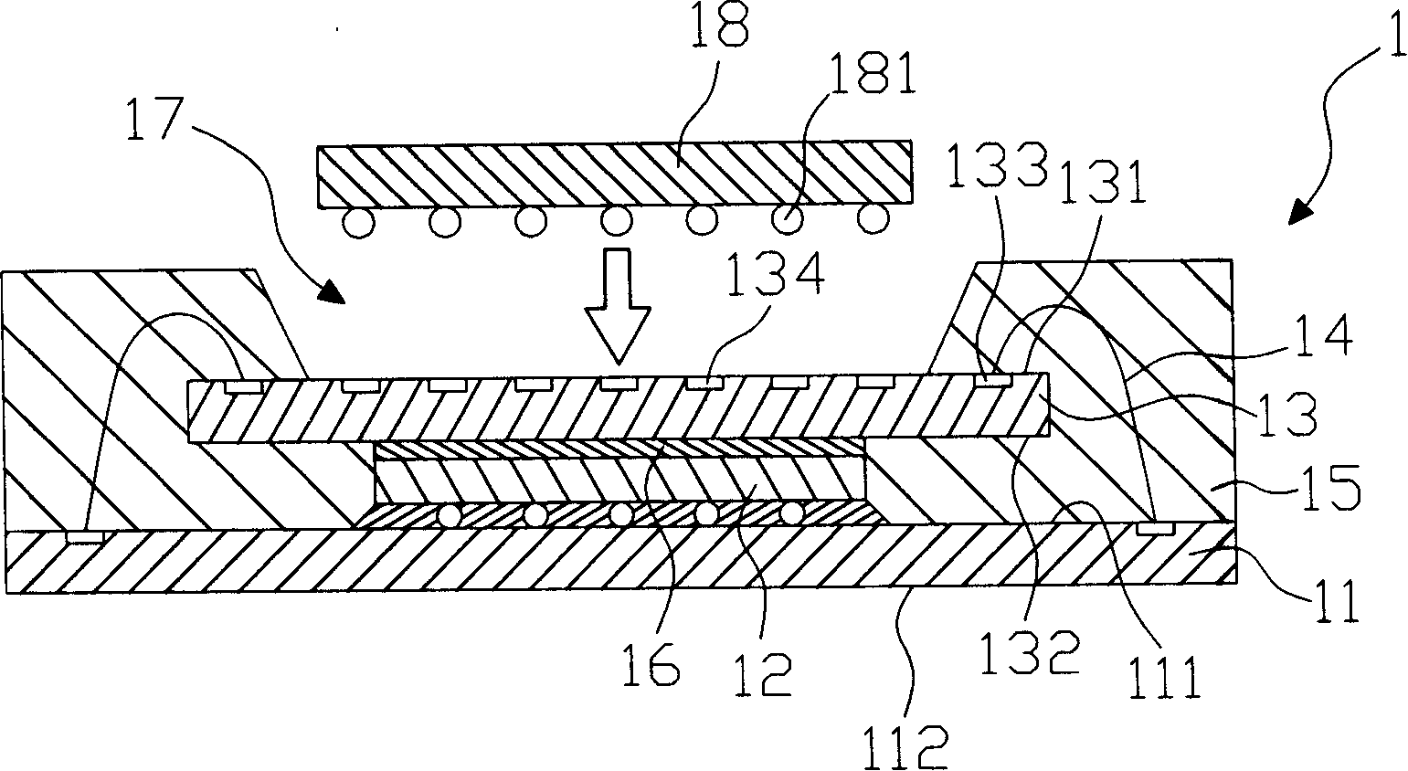
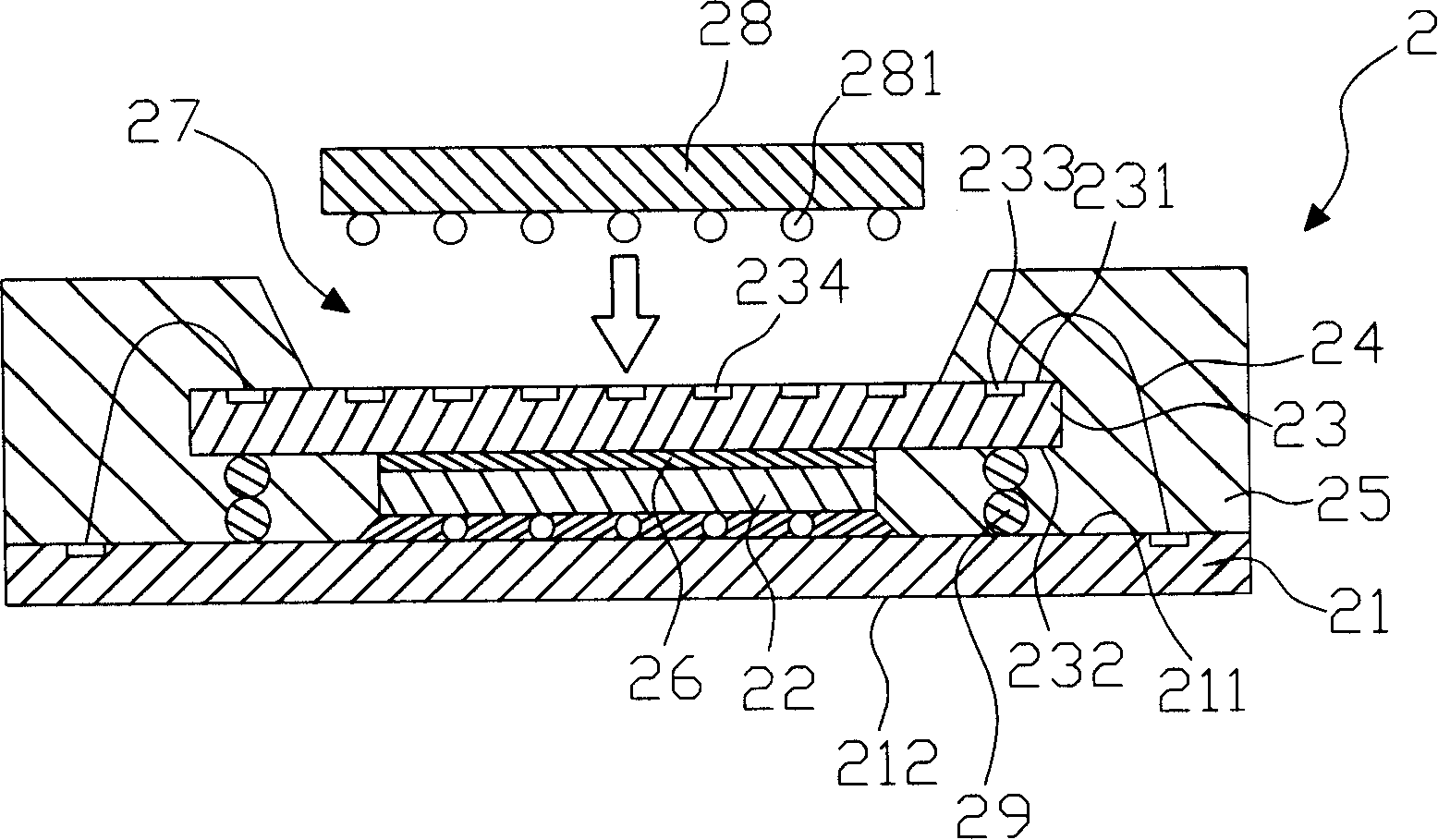
[0014] refer to figure 2 , shows a schematic cross-sectional view of the first embodiment of the stackable semiconductor package structure of the present invention. The stackable semiconductor package structure 2 includes a first substrate 21, a chip 22, a second substrate 23, several supporting components (that is, several dummy solder balls 29, which do not have the function of electrical connection) and a layer Sealing material 25. The first substrate 21 has a first surface 211 and a second surface 212 . The chip 22 is located on the first surface 211 of the first substrate 21 and is electrically connected to the first surface 211 of the first substrate 21 . In this embodiment, the chip 22 is attached to the first surface 211 of the first substrate 21 in a flip-chip manner.

[0015] The second substrate 23 is adhered on the chip 22 by a layer of adhesive layer 26, the second substrate 23 has a first surface 231 and a second surface 232, wherein the first surface 231 has...


PUM


Abstract

The invention relates to a stacking type semiconductor package structure which comprises a first substrate, a chip, a second substrate, a plurality of second conducting wires, a plurality of support components and seal gum material, wherein the chip is positioned on and in electrical connection with one surface of the first substrate; the second substrate with the area more than that of the chip is positioned above the chip; moreover, the second substrate is in electrical connection with the first substrate by means of the second conducting wires; the support components are positioned between the first substrate and the second substrate to support the second substrate; the seal gum material is coated on one surface of the first substrate, the chip, the second conducting wires, the support components and part of the second substrate with one surface of the second substrate exposed. Therefore, the suspended part of the second substrate does not swing or shake during wire bonding operation.

Description

technical field [0001] The present invention relates to a stackable semiconductor packaging structure, in particular to a stackable semiconductor packaging structure using a support component as support. Background technique [0002] refer to figure 1 , showing a schematic cross-sectional view of a conventional stackable semiconductor package structure. The conventional stackable semiconductor package structure 1 includes a first substrate 11 , a chip 12 , a second substrate 13 , several wires 14 and a layer of sealing material 15 . The first substrate 11 has a first surface 111 and a second surface 112 . The chip 12 is flip-chip attached to the first surface 111 of the first substrate 11 . The second substrate 13 is adhered on the chip 12 by a layer of adhesive layer 16, the second substrate 13 has a first surface 131 and a second surface 132, wherein the first surface 131 has a plurality of first soldering pads 133 and several second welding pads 134. The area of ​​th...

Claims


Application Information

Patent Timeline
Patent Type & Authority Applications(China)
IPC IPC(8): H01L25/00H01L25/16H01L23/488H01L23/31
CPCH01L2924/1815H01L2224/73204H01L2224/48091H01L2224/73265
Inventor 卢勇利翁国良
Owner ADVANCED SEMICON ENG INC
Features
  • R&D
  • Intellectual Property
  • Life Sciences
  • Materials
  • Tech Scout
  • Unparalleled Data Quality
  • Higher Quality Content
  • 60% Fewer Hallucinations
Learn More