Method for removing photoresist graphical in forming process of dual embedded structure

A dual damascene structure and photoresist technology, applied in the processing of photosensitive materials, electrical components, semiconductor/solid-state device manufacturing, etc., can solve the problems of complex process, increased dielectric constant, and easy damage, and simplify the removal process. , the effect that the dielectric constant does not change

Active Publication Date: 2008-06-18
SEMICON MFG INT (SHANGHAI) CORP +1
View PDF1 Cites 12 Cited by
  • Summary
  • Abstract
  • Description
  • Claims
  • Application Information

AI Technical Summary

Problems solved by technology

This process is not only complicated, but also easily destroys the low dielectric constant dielectric layer 16, which increases the dielectric constant of this layer and affects device performance.
Moreover, since the material of the sacrificial layer is mostly BARC or silicon-rich polymer, it is easy to generate polymer residue 23 on the inner wall of the connection hole of the dielectric layer 16 when etching the sacrificial layer, which seriously affects the subsequent process.

Method used


Image

  • Method for removing photoresist graphical in forming process of dual embedded structure
  • Method for removing photoresist graphical in forming process of dual embedded structure
  • Method for removing photoresist graphical in forming process of dual embedded structure

Examples


Embodiment Construction

[0037] In order to make the above objects, features and advantages of the present invention more comprehensible, specific implementations of the present invention will be described in detail below in conjunction with the accompanying drawings.

[0038] In the following description, numerous specific details are set forth in order to provide a thorough understanding of the present invention. However, the present invention can be implemented in many ways other than those described here, and those skilled in the art can make similar extensions without departing from the connotation of the present invention. Accordingly, the invention is not limited to the specific implementations disclosed below.

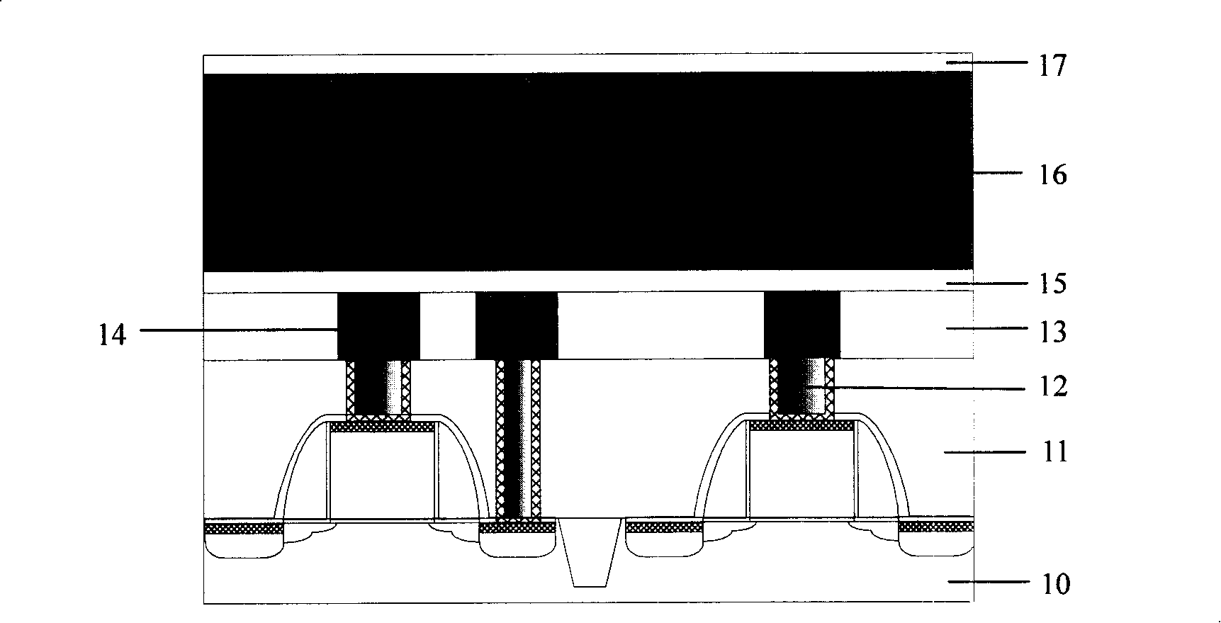
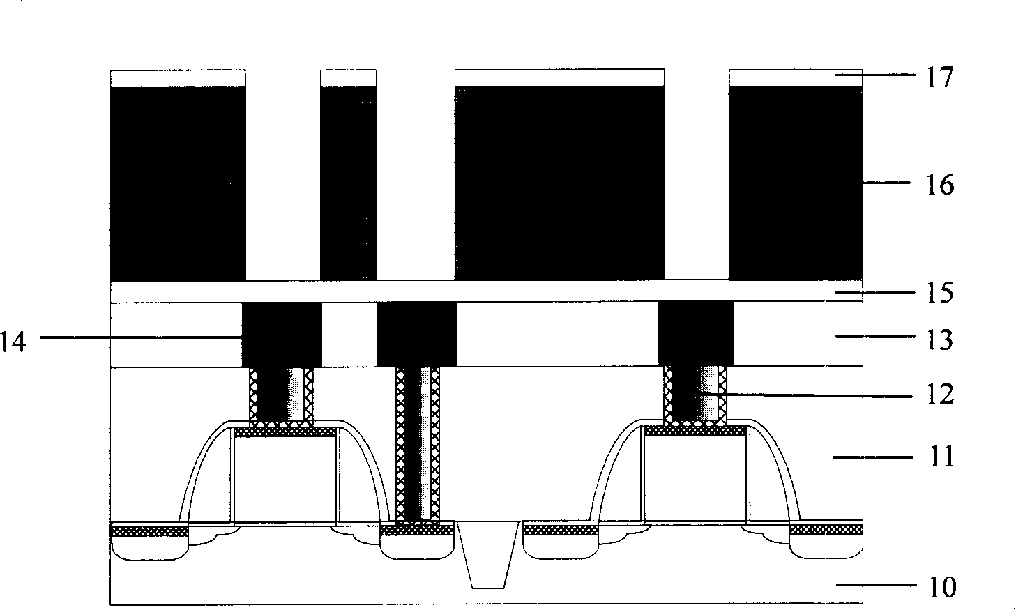
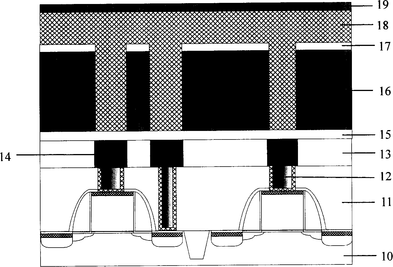
[0039] Such as Figure 6 As shown, a semiconductor substrate 10, the substrate 10 is silicon or silicon germanium (SiGe) of single crystal, polycrystalline or amorphous structure, may also be silicon on insulator (SOI), and may also include other materials, such as antimony Indium, l...


PUM


Abstract

The invention provides a removing method for a photo resist image in the forming process of a double inlaying structure; the forming process of the double inlaying structure comprises the following steps: a semiconductor substrate with a preformed semiconductor device is provided; a metal interconnecting line layer with a surface which is provided with a dielectric layer is formed on the substrate; connecting holes are etched in the dielectric layer; a sacrificial layer and a hard mask layer are deposited; a bottom anti-reflecting layer and a photo-resist layer are coated and patterned to form the photo resist image; oxy plasma incinerates and removes the bottom anti-reflecting layer and the photo-resist layer. The removing method of the invention can simplify the removing process and prevent the dielectric layer with a low dielectric constant from being damaged.

Description

technical field [0001] The invention relates to the technical field of semiconductor manufacturing, in particular to a method for removing photoresist patterns during the formation of a dual damascene structure. Background technique [0002] Today's semiconductor device manufacturing technology is developing rapidly, semiconductor devices already have a deep submicron structure, and integrated circuits contain a huge number of semiconductor components. In such large-scale integrated circuits, high-performance, high-density connections between components are not only interconnected in a single interconnect layer, but also interconnected between multiple layers. Therefore, a multilayer interconnection structure is generally provided in which a plurality of interconnection layers are stacked on each other with an interlayer insulating film interposed therebetween for connecting semiconductor elements. Especially the multi-layer interconnect structure formed by the dual-damasce...

Claims


Application Information

Patent Timeline
Patent Type & Authority Applications(China)
IPC IPC(8): H01L21/768G03F7/36
Inventor 王荣王琪宁先捷
Owner SEMICON MFG INT (SHANGHAI) CORP
Why Eureka
Try Eureka