
Method for monitoring low temperature rapid hot technics

A thermal process and low-temperature technology, which is applied in electrical components, semiconductor/solid-state device manufacturing, circuits, etc., can solve problems such as inability to measure, waste of wafers, and knowing the effectiveness of thermal processes, etc.

Inactive Publication Date: 2008-06-25
GRACE SEMICON MFG CORP
View PDF0 Cites 6 Cited by
  • Summary
  • Abstract
  • Description
  • Claims
  • Application Information

AI Technical Summary

Problems solved by technology

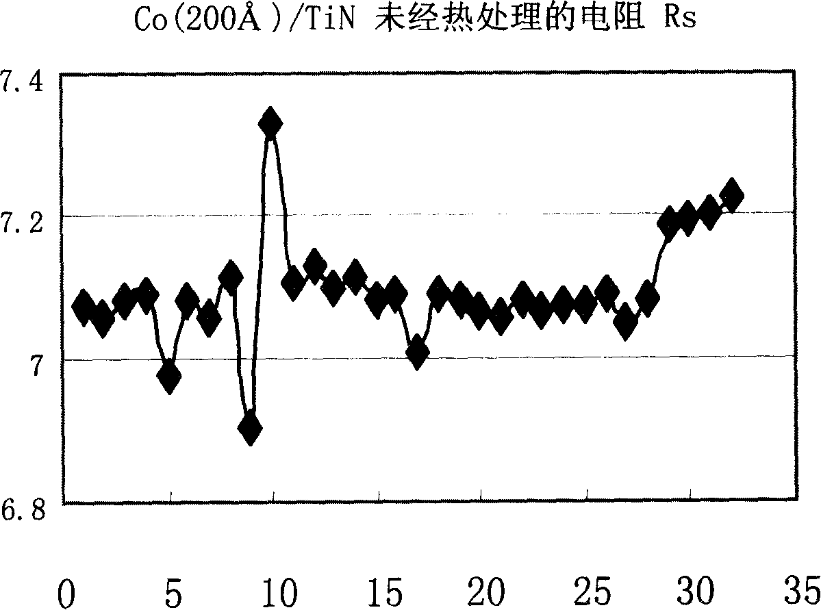
[0004] However, the method used to monitor the state of the low-temperature rapid thermal process is to form a silicide layer on the wafer with a thickness of 100 cobalt metal layer with a thickness of 200 The monitoring layer of the titanium nitride layer is used for process temperature control, but the thickness is 100 When the cobalt metal layer is used for monitoring, the measured resistance value is easily affected by the surface state of the wafer, resulting in a large difference in the resistance value picked up from various places on the wafer, which is about 4.44. This situation will lead to subsequent heat treatment. After the monitoring layer, it is impossible to accurately measure the resistance value of the monitoring layer to know the effect of the thermal process, resulting in unnecessary waste of wafers
[0005] Therefore, the present invention proposes a method for monitoring the low-temperature rapid thermal process to solve the problem that the low-temperature rapid thermal process is not easy to monitor, and further reduces unnecessary process cost waste caused by monitoring failure.

Method used


Image

  • Method for monitoring low temperature rapid hot technics
  • Method for monitoring low temperature rapid hot technics
  • Method for monitoring low temperature rapid hot technics

Examples


Embodiment Construction

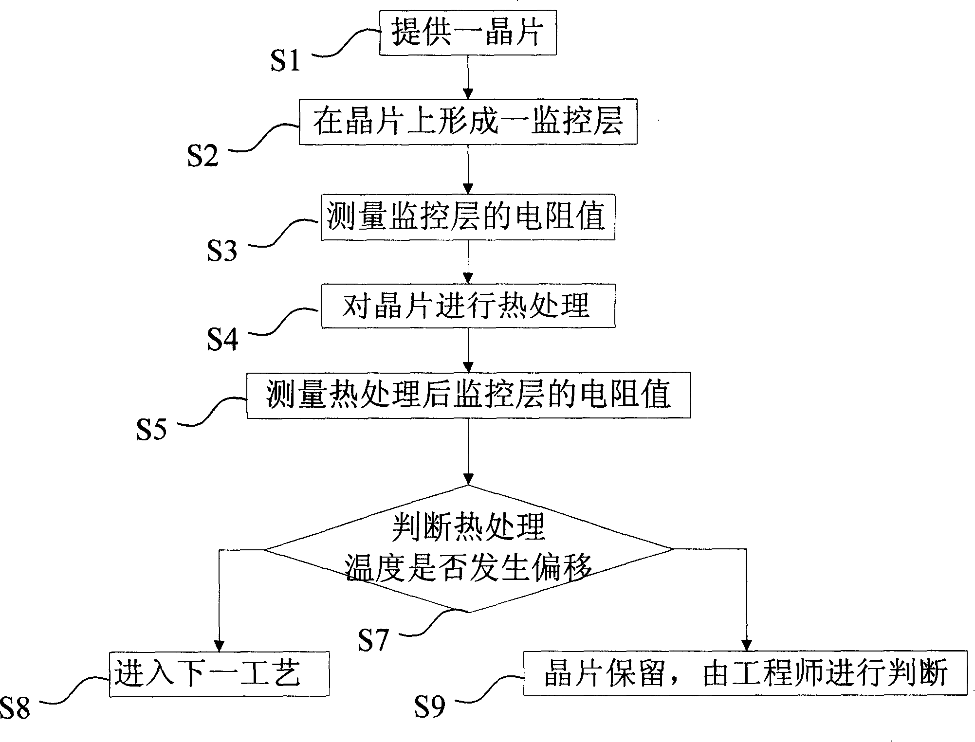
[0022] A method of monitoring low temperature rapid thermal processes, see figure 1 and figure 2 , figure 1 A side view of the wafer after depositing the monitor layer, while figure 2 It is a flow chart of the steps, first as in step S1: a wafer is provided, then as in step S2: a monitoring layer is formed on the wafer 10, the formation method of the monitoring layer is first with low pressure chemical vapor deposition (LPVCD) or with silicon ions or germanium The ions are ion-implanted as dopant ions, and a silicide layer 12 is formed on the wafer 10, wherein the wafer 10 can be a wafer, and then a silicide layer 12 with a thickness of 200 μm is formed on the silicide layer 12. Cobalt metal layer 14, with a thickness of 200 Titanium nitride layer 16, measuring the resistance value of the monitoring layer is as in step S3: judging whether the resistance value is within the upper and lower maximum error range of the monitoring layer resistance value. Of course, this erro...


PUM


Abstract

The invention provides a method of monitoring the low temperature rapid thermal process, a monitoring layer comprising a silicide layer, a cobalt metallic layer with thickness of 200 and a titanium nitride layer with thickness of 200 formed on the wafer is utilized, and the stability of the low temperature rapid thermal process is monitored through measuring the electrical resistance value of the monitoring layer; therefore, the effect of the low temperature rapid thermal process can be obtained, and the defect that the prior cobalt metallic layer with thickness of 100 easily occurs the monitoring failure because of the surface state of the wafer is solved.

Description

technical field [0001] The invention relates to a method for monitoring a low-temperature rapid thermal process, in particular to a method with a thickness of 200 Cobalt metal silicide method to monitor low temperature rapid thermal process. Background technique [0002] Low temperature thermal process is a very common process technology in metallurgical material process. Its purpose is to eliminate the internal stress accumulated by defects in materials (especially metal materials). The method used is to place the material at an appropriate high temperature for a period of time, and use thermal energy to enable the atoms in the material to rearrange the lattice positions to reduce the defect density (DefectDensity) in the material. [0003] The main defects of the material come from the grain boundary (Grain Boundary), dislocation (Dislocation) and various point defects (Point Defects), etc. The defect or structure of the material plays a decisive role in the electrical ...

Claims


Application Information

Patent Timeline
IPC IPC(8): H01L21/00H01L21/66
Inventor 金桂东江瑞星缪敦耀高玉歧
Owner GRACE SEMICON MFG CORP
Learn More