Inner lining of wafer processing chamber and wafer processing chamber containing said inner lining

A wafer processing and lining technology, which is applied in gaseous chemical plating, coating, electrical components, etc., can solve the problems of limiting the uniformity of the gas flow field on the surface of the wafer, and improve the uniformity of the flow field and increase the airflow passing area. Effect

Active Publication Date: 2008-06-25
BEIJING NAURA MICROELECTRONICS EQUIP CO LTD
View PDF0 Cites 5 Cited by
  • Summary
  • Abstract
  • Description
  • Claims
  • Application Information

AI Technical Summary

Problems solved by technology

[0004] In the prior art, the shielding plate 4 is generally perpendicular to the axis of the lining. When the gas flow flows through the shielding hole 1 in this lining structure, due to the limitation of the area of ​​the gas flow, the gas flow on the surface of the wafer is limited. Improvement of flow field uniformity

Method used


Image

  • Inner lining of wafer processing chamber and wafer processing chamber containing said inner lining
  • Inner lining of wafer processing chamber and wafer processing chamber containing said inner lining
  • Inner lining of wafer processing chamber and wafer processing chamber containing said inner lining

Examples


Embodiment Construction

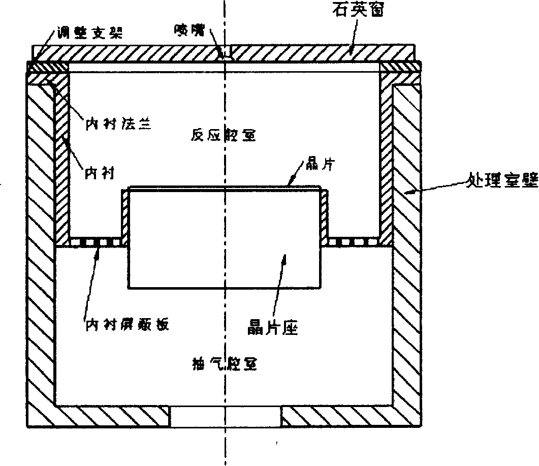
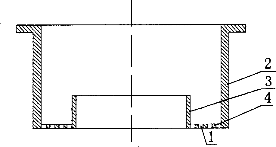
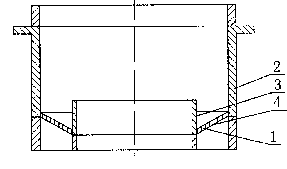
[0022] The lining of the wafer processing chamber of the present invention, its preferred embodiment is as image 3 As shown, it includes an inner side wall 3 and an outer side wall 2, the inner side wall 3 and the outer side wall 2 are connected by a shielding plate 4, and the shielding plate 4 is obliquely connected to the side wall. It may be that the part where the shielding plate 4 is connected to the outer wall 2 is higher than the part where it is connected to the inner wall 3 ;

[0023] The included angle between the shielding plate 4 and the liner axis is 5-80°, preferably 5, 20, 45, 60, 80°, etc., preferably 20-60°.

[0024] The shielding plate 4 is provided with a shielding hole 1 which communicates up and down. The shape of the cross-section of the shielding hole 1 is circular, elliptical or polygonal, or other required shapes.

[0025] The direction of the shielding hole 1 can be parallel to the axis of the lining; it can also be perpendicular to the shielding pl...


PUM


Abstract

The invention discloses a chip processing chamber liner and a chip processing chamber comprising the liner. The invention comprises a inside wall and a lateral wall , the inside wall l is connected with the lateral wall through a screen board, and the shield plate is obliquely connected with the sidewall. The slope area has obvious increment compared with that of the plane area, therefore a slope structure can increase the quantity or the area of the shield openings , namely, the slope structure can increase the passing area of airflow. According to requirements, the inclined angle of the shield plate and the direction of the shield opening can be chosen, so as to reach the purpose of the uniformity of airflow field on the surface of the chip. The invention is mainly applied in the semiconductor chip processing chambers, and also is applied in other similar cavities.

Description

technical field [0001] The invention relates to a semiconductor processing equipment component, in particular to a wafer processing chamber and its lining. Background technique [0002] In semiconductor silicon wafer processing, etching or other processing processes on wafers are usually performed in a processing chamber. The process gas is ionized into plasma in the processing chamber to process the wafer. While the plasma is processing the silicon wafer, it will also cause pollution or damage to the wall of the processing chamber, which will affect the processing technology of the wafer. Such as figure 1 As shown, the processing chamber generally adopts a lining structure to protect the wall of the processing chamber. There is a quartz window above the treatment chamber, and the nozzle on the quartz window adopts a trumpet-shaped structure, and an adjustment bracket is provided between the quartz window and the treatment chamber wall, and the lining covers the inner sur...

Claims


Application Information

Patent Timeline
Patent Type & Authority Applications(China)
IPC IPC(8): H01L21/00H01L21/3065H01L21/205H01L21/67C23C16/00C23F4/00H01J37/32H05H1/00
Inventor 林盛
Owner BEIJING NAURA MICROELECTRONICS EQUIP CO LTD
Why Eureka
Try Eureka