Organic electroluminescent display device and method of manufacture

An electroluminescence display and display device technology, applied in semiconductor/solid-state device manufacturing, electrical solid-state devices, electrical components, etc., can solve problems such as energy level mismatch between RGB three colors, affecting device performance, etc., and achieve high yield , The effect of simple process and low production cost

Inactive Publication Date: 2008-07-02
INESA ELECTRON
View PDF0 Cites 7 Cited by
  • Summary
  • Abstract
  • Description
  • Claims
  • Application Information

AI Technical Summary

Problems solved by technology

Therefore, when the RGB three colors are in the same display, it will inevitably lead to the mismatch of energy levels among the three RGB colors, which will affect the performance of the device.

Method used


Image

  • Organic electroluminescent display device and method of manufacture
  • Organic electroluminescent display device and method of manufacture
  • Organic electroluminescent display device and method of manufacture

Examples


Embodiment Construction

[0024] The embodiments of the present invention will be described in further detail below in conjunction with the accompanying drawings, but the present embodiments are not intended to limit the present invention, and any similar structures and similar changes of the present invention should be included in the protection scope of the present invention.

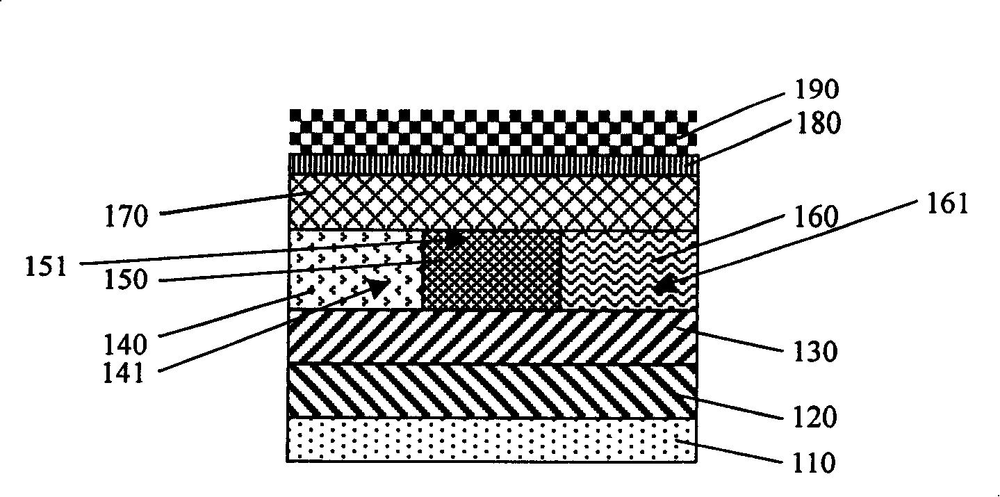
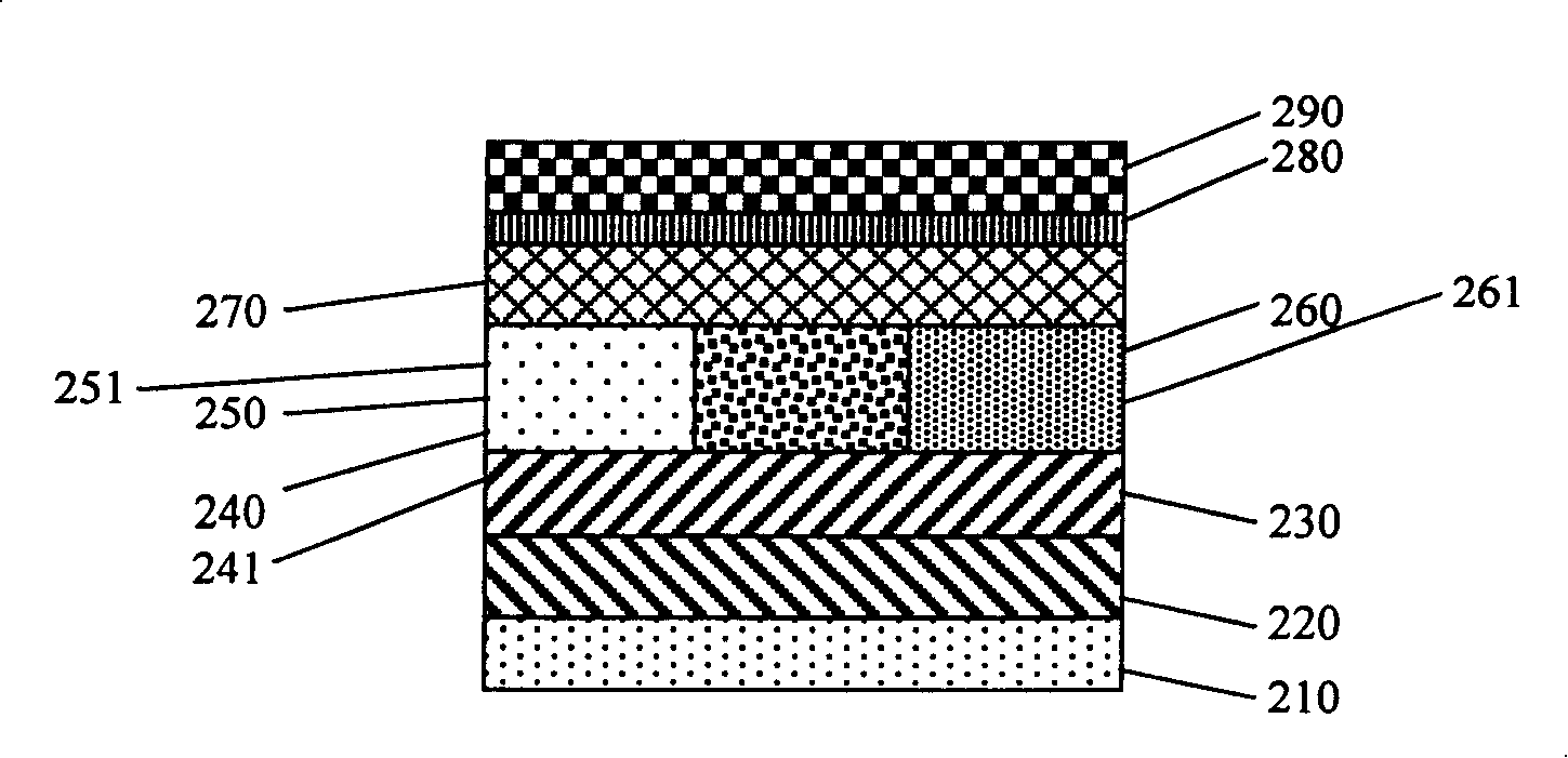
[0025] see figure 2 As shown, an organic electroluminescent display device provided by the embodiment of the present invention includes a cathode layer 290 from top to bottom, an electronic organic functional layer including an electron injection layer 280 and an electron transport layer 270, and RGB three-color luminescence layer, a hole organic functional layer comprising a hole transport layer 230 and a hole injection layer 220, and an anode layer 210; it is characterized in that the light-emitting layer adopts the same wide-level light-emitting host (host) material, ( There are at least two layers containing the same host...


PUM


Abstract

The invention discloses an organically electroluminescent display device and a manufacture method thereof, which relates to a technical field of an electron display device. The technical issues to be solved are accelerating luminescent efficiency of the device and improving stability of the device. The luminescent device comprises a cathode layer, an electron organic-function layer including an electron injection layer and an electron transport layer, a luminescent layer with three colors of the red, green and blue (RGB), a hole organic-function layer including a hole transport layer and a hole injection layer and an anode layer from the upper part to the lower part. The invention is characterized in that in the luminescent layer, luminescent main material with same wide energy level is adopted by at least two primary colors; at the same time, luminescent guest material with different primary colors are respectively and correspondingly doped to realize the organically electroluminescent display with different colors. The invention solves the energy level matching problems caused by adopting different material in the three primary colors RGB in the prior art, accelerates the luminescent efficiency, and improves the stability of the device; the invention has the advantages of simple process, low cost and high yield.

Description

technical field [0001] The invention relates to the technical field of electronic display devices, in particular to the technology of an organic electroluminescence display device structure and a manufacturing method thereof. Background technique [0002] At present, the structure of organic electroluminescent devices is generally composed of transparent conductive film, hole injection layer (HIL), hole transport layer (HTL), light emitting layer (EML), electron transport layer (ETL) and electron injection layer (EIL). with the cathode. The light-emitting layer (EML) currently used is usually doped by a certain ratio of host (host) material and guest (dopant) light-emitting material. Usually, the guest (dopant) light-emitting material accounts for 0.1% to 15% of the host material. [0003] The full-color device structure of the prior art is as figure 1 shown. The red light emitting layer 140 , the green light emitting layer 150 and the blue light emitting layer 160 are lo...

Claims


Application Information

Patent Timeline
Patent Type & Authority Applications(China)
IPC IPC(8): H01L27/32H01L51/50H01L51/54H01L51/56H01L21/82
Inventor 徐洪光余峰
Owner INESA ELECTRON
Why Eureka
Try Eureka