

An organic thin film transistor and its making method
An organic thin film and manufacturing method technology, which is applied in semiconductor/solid-state device manufacturing, electric solid-state devices, semiconductor devices, etc., can solve the problems of reduced component performance characteristics, poor adhesion, etc., to improve component performance, save costs, avoid The effect of component damage
- Summary
- Abstract
- Description
- Claims
- Application Information
AI Technical Summary
Problems solved by technology
Method used
Image

Examples
Embodiment Construction
[0030] Figure 1A to Figure 1D It is a schematic cross-sectional flow diagram of a method for manufacturing an organic thin film transistor according to an embodiment of the present invention.
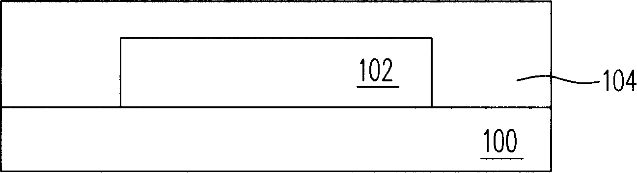
[0031] Please refer to Figure 1A , providing a substrate 100 . The substrate 100 is, for example, a glass substrate or a plastic substrate. Then, a gate 102 is formed on the substrate 100 . The material of the gate 102 is, for example, chromium (Cr), aluminum (Al), aluminum neodymium (AlNd), or other suitable metals or metal alloys. The forming method of the gate 102 is, for example, chemical vapor deposition (CVD) or physical vapor deposition (PVD). Of course, the material of the gate 102 can also be, for example, gold nanoparticles, silver nanoparticles, palladium nanoparticles, copper nanoparticles or other suitable metal nanoparticles, and its formation method is, for example, using a transfer printing method (printing) or an inkjet method. (ink-jet).
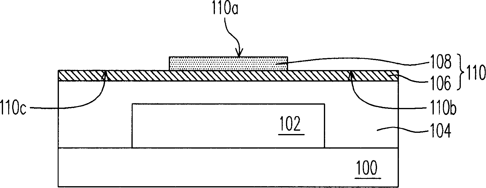
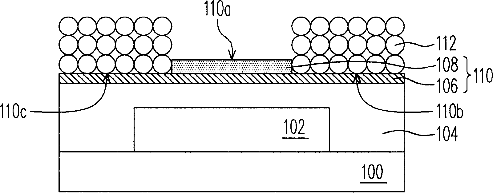
[0032] Then, please co...
PUM
 Abstract
Description
Claims
Application Information