Method for promoting electrostatic charge dissipation on semiconductor chip

An electrostatic charge and semiconductor technology, applied in the field of semiconductor wafer production, can solve problems such as the inability to take out the wafer smoothly, secondary damage to the wafer surface, damage to the thimble and the manipulator, etc., to shorten the dissipation time, promote dissipation, and increase productivity.

Active Publication Date: 2008-07-16
BEIJING NAURA MICROELECTRONICS EQUIP CO LTD
View PDF0 Cites 9 Cited by
  • Summary
  • Abstract
  • Description
  • Claims
  • Application Information

AI Technical Summary

Problems solved by technology

This method only delays waiting while maintaining the plasma, and the release time is longer, which reduces the productivity, and the existence of the plasma for too long may cause secondary damage to the wafer surface that has completed the process
[0008] And if the electrostatic charge on the semiconductor wafer is not completely dissipated, the operation may occur, the wafer may jump or shift when the thimble is raised, resulting in the failure to take out the wafer smoothly, and it may even damage the thimble and the manipulator.

Method used


Image

  • Method for promoting electrostatic charge dissipation on semiconductor chip
  • Method for promoting electrostatic charge dissipation on semiconductor chip
  • Method for promoting electrostatic charge dissipation on semiconductor chip

Examples


Embodiment 1

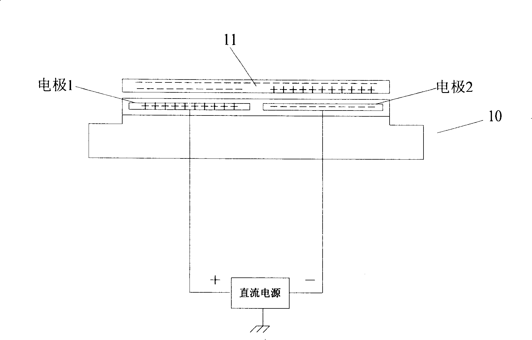
[0031] Embodiment 1: What provide electric potential for two electrodes on the double-electrode electrostatic chuck 10 are two DC power supplies whose output can be switched positive and negative, such as figure 2 As shown, the two DC power supplies are connected in series, and each has an output terminal connected to the electrode.

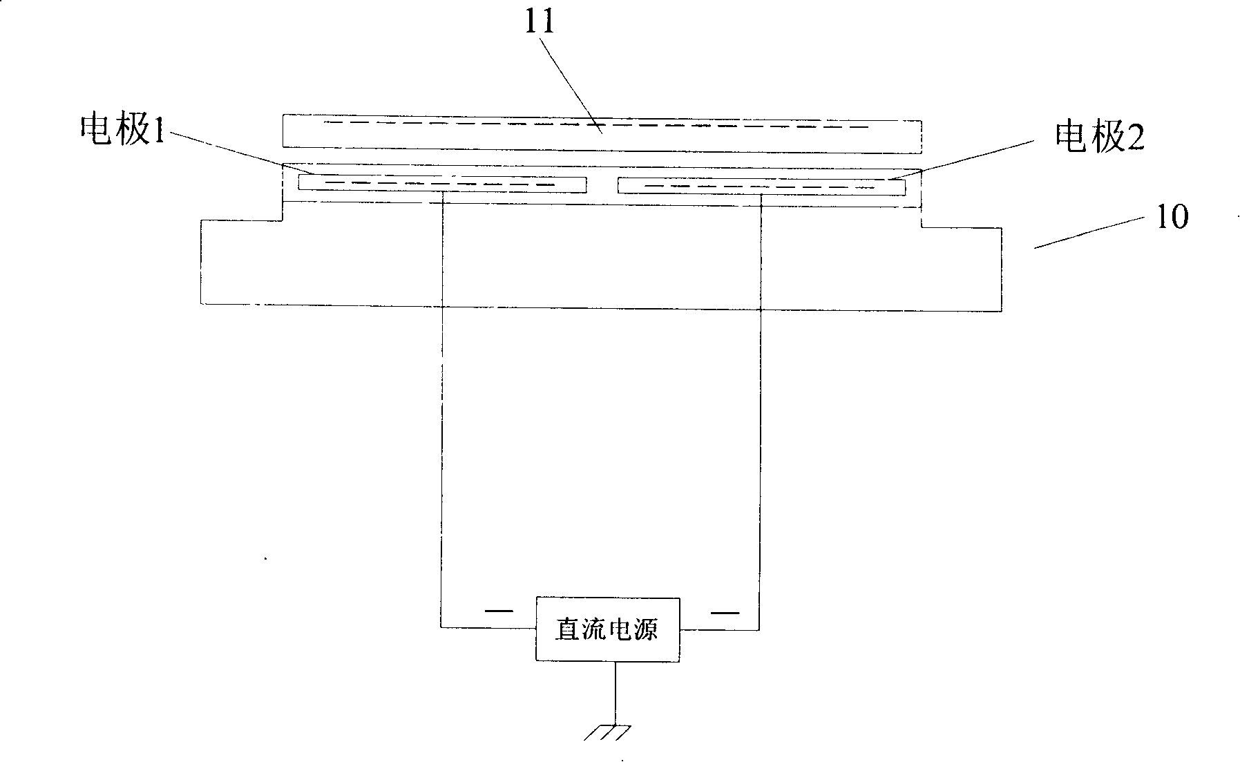
[0032] Such as Figure 4 Shown is the operation flow for releasing a semiconductor wafer from a two-electrode electrostatic chuck. First, in the process, let the electrode 1 of the two-electrode electrostatic chuck 10 be at a positive potential, and the electrode 2 be at a negative potential, and the semiconductor wafer 11 will be attracted on the surface of the two-electrode electrostatic chuck 10, thereby the semiconductor wafer is carried out correspondingly. Process processing or transmission; when the semiconductor wafer starts to be released, change the output polarity of the two DC power supplies, so that the electrode 1 of the double-el...

Embodiment 2

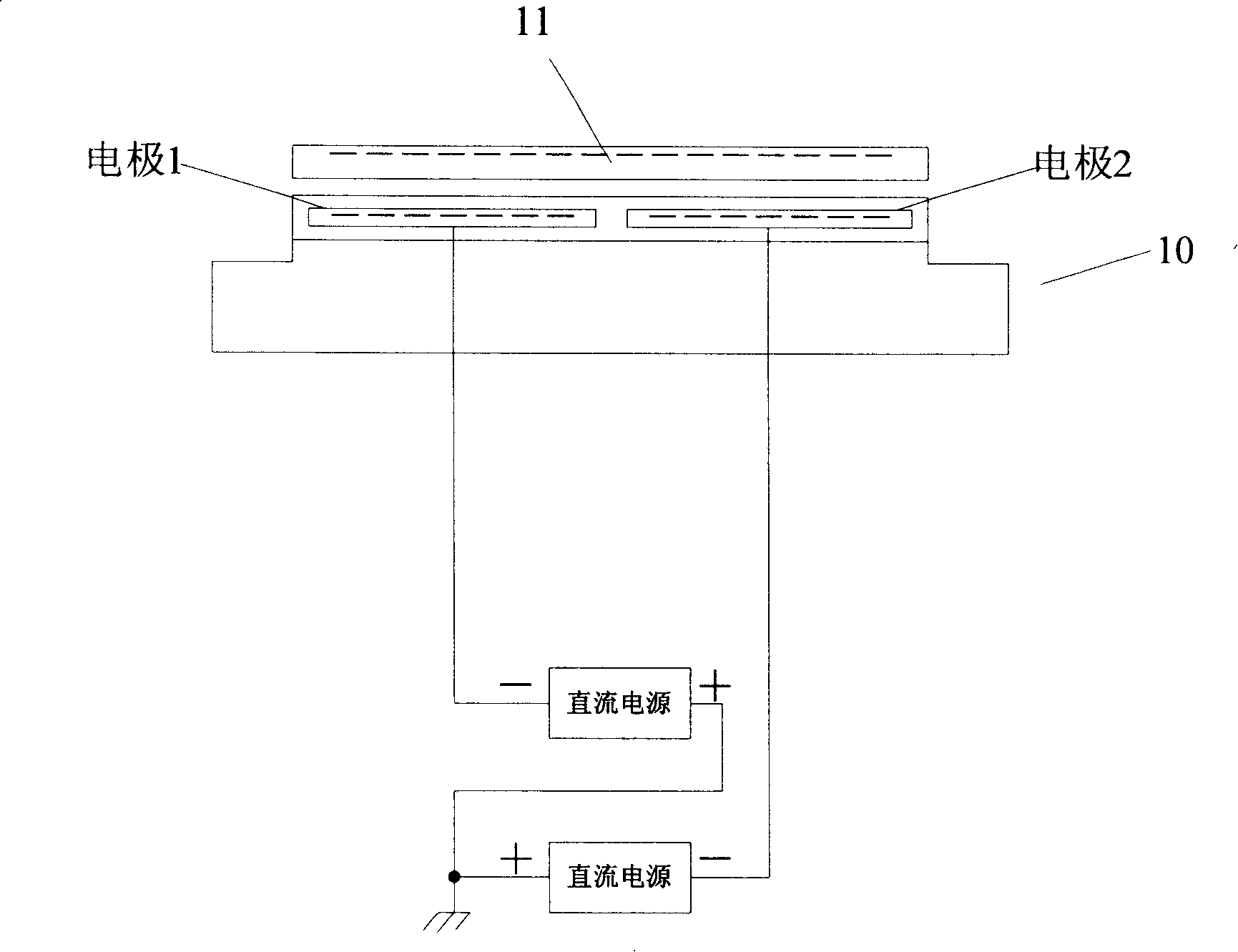
[0036] Embodiment 2: It is a DC power supply whose output can be positive and negative exchanged for the two electrodes on the double-electrode electrostatic chuck 10 to provide potential, such as image 3 As shown, the outputs at both ends are connected to the two electrodes respectively.

[0037] Such as Figure 4Shown is the operation flow for releasing a semiconductor wafer from a two-electrode electrostatic chuck. First, in the process, let the electrode 1 of the two-electrode electrostatic chuck 10 be at a positive potential, and the electrode 2 be at a negative potential, and the semiconductor wafer 11 will be attracted on the surface of the two-electrode electrostatic chuck 10, thereby the semiconductor wafer is carried out correspondingly. Process processing or transmission; when the semiconductor wafer starts to be released, change the output polarity of the DC power supply, so that the electrode 1 of the double-electrode electrostatic chuck is at a negative potenti...


PUM


Abstract

The invention provides a method for accelerating the dissipation of electrostatic charge on a semi-conductor chip, which in details is that: When the semi-conductor chip is released from the double-pole electrostatic chuck, negative electric potential is applied at the two poles of the double-pole electrostatic chuck so as to accelerate the dissipation of the additional electrostatic charge on the semi-conductor chip. With the implementation of the technical proposal, the dissipation of the additional electrostatic charge on the semi-conductor chip can be accelerated notably, which reduces the dissipation time of the electrostatic charge and thus the release time of the semi-conductor chip as well and improves the production rate. In addition, the invention is easy to operate and strong in reliability without addition of any mechanical structure.

Description

technical field [0001] The invention relates to the field of semiconductor wafer production, in particular to a method for promoting the dissipation of electrostatic charge on the semiconductor wafer. Background technique [0002] At present, with the rapid development of electronic technology, people have higher and higher requirements for the integration of integrated circuits, which requires enterprises that produce integrated circuits to continuously improve the processing capacity of semiconductor wafers. Plasma devices are widely used in fabrication processes for fabricating integrated circuits (ICs) or MEMS devices. Among them, inductively coupled plasma (ICP) is widely used in etching and other processes. Under low pressure, the reactive gas is excited by radio frequency power to generate ionization to form a plasma. The plasma contains a large number of active particles such as electrons, ions, excited atoms, molecules and free radicals. These active reactive group...

Claims


Application Information

Patent Timeline
Patent Type & Authority Applications(China)
IPC IPC(8): H01L21/00H01L21/67H01L21/683H01L21/306
Inventor 刘利坚
Owner BEIJING NAURA MICROELECTRONICS EQUIP CO LTD
Why Eureka
Try Eureka