Broad band charge amplifier and design method thereof

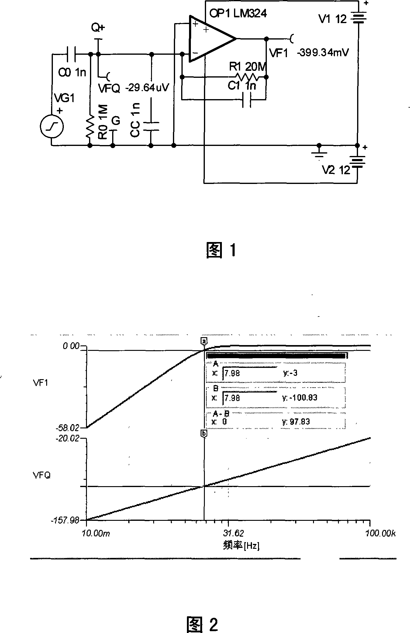
A charge amplifier, broadband technology, applied in charge amplifiers, improving amplifiers to expand bandwidth, etc., can solve problems such as the meaninglessness of resistance devices, the reduction of transmission characteristics to -58dB, and the reduction of insulation resistance.

Active Publication Date: 2008-07-23
北京唐智科技发展有限公司
View PDF0 Cites 7 Cited by
  • Summary
  • Abstract
  • Description
  • Claims
  • Application Information

AI Technical Summary

Problems solved by technology

[0009] The problem is: when the frequency is as low as f0=7.98Hz, the transmission characteristic of the known charge amplifier (as shown in Figure 2) drops to -3.01dB, and this frequency f0 is called "the corner frequency". Hz, the transfer characteristic drops to -58dB
Although modern high-performance op amps can operate at R 1 The working point of the charge...

Method used


Image

  • Broad band charge amplifier and design method thereof
  • Broad band charge amplifier and design method thereof
  • Broad band charge amplifier and design method thereof

Examples


Embodiment 1

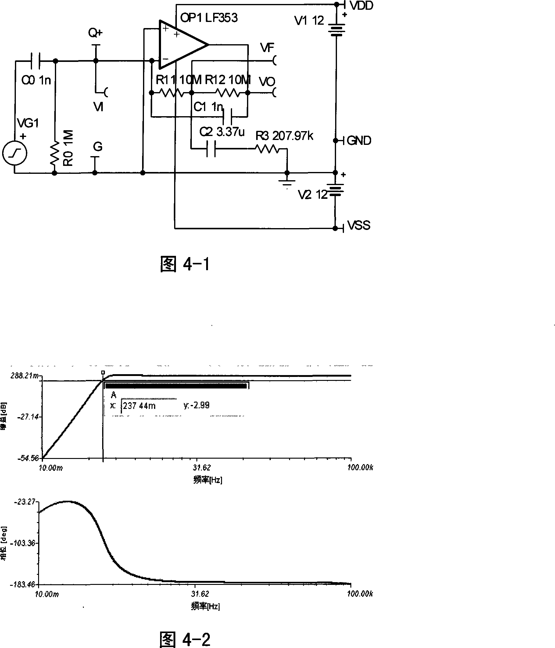
[0097] Embodiment 1, Feedback Bypass Low Frequency Single-Ended Charge Amplifier

[0098] The principle of the feedback bypass type low-frequency charge amplifier technology proposed by the present invention is to connect the capacitor in series with the resistor C 2 +R 3 The branch puts the resistor R 11 with resistor R 12 The connection point V F The AC potential of the resistor R is pulled towards the potential of the reference point G without adding appreciable phase shift, causing the resistor R 11 Same as op amp OP 1 The effect of AC grounding at the negative input terminal of the op amp is to fully reduce the negative input terminal of the op amp from the op amp OP 1 output, except C 1 External AC negative feedback, thereby improving the low-frequency frequency response.

[0099] This broadband charge amplifier (see accompanying drawings 4-1, 4-2) contains an operational amplifier OP 1 , resistor R 11 , R 12 , R 3 , capacitor C 1 、C 2 , op amp OP 1 The pos...

Embodiment 2

[0155] Embodiment 2 is a single-supply single-ended input broadband charge amplifier

[0156] As shown in Figure 7, a single-power single-ended input wide-band charge amplifier is used for occasions where there is only a single power supply, and is characterized in that it contains an operational amplifier OP 1 , O P 2. Resistor R 1 ~R 3 , R 11 , R 12 , capacitor C 1 ~C 3 , the positive power supply terminal of each op amp is connected to the positive power supply terminal V DD , the ground wire GND of the negative power supply terminal of the op amp, and the resistor R 1 One end of the ground, the other end of the op amp OP 2 the positive input and the resistor R 2 one end of the capacitor C 3 One end of the capacitor C 3 The other end of the ground is GND, the resistor R 2 The other end is connected to the positive power supply terminal V DD , op amp OP 2 The output terminal of the output terminal is connected to its negative input terminal, and the level equal...

Embodiment 3

[0157] Embodiment 3 is a differential input broadband charge amplifier

[0158] A kind of differential input broadband charge amplifier as shown in accompanying drawing 8, the purpose is in order to improve the anti-jamming capability, it is characterized in that the input terminal Q+, Q- and reference terminal G of the charge signal source are provided, and the Q+ signal is provided with A positive charge converter for charge-to-voltage conversion and a negative charge converter for charge-to-voltage conversion of the Q-signal; the positive charge converter contains an operational amplifier OP 1 , resistor R 11 , R 12 , the feedback capacitor C 11 , op amp OP 1 The positive input terminal is connected to the reference terminal G, the negative input terminal is connected to the positive charge input terminal Q+, and also connected to the resistor R 11 One end of the resistor R 11 The other end of the resistor R 12 One end of the resistor R 12 The other end of the op amp...


PUM


Abstract

A wide frequency band charge amplifier is used to change charge voltage, which is characterized in that a feedback resistance which is jumped between a negative input end and output end of an operational amplifier to a R11, R12 series circuits in the widely-known charge amplifier circuit, a reference end G is connected to a feedback by-passing branch through a connecting point of the R12, the feedback by-passing branch is formed through connecting R3 and C2 in series, when R11=R12=R, the feedback by-passing branch which is connected can lead a breaking frequency f0 of a charge amplifier output end VO without the feedback by-passing branch to reduce to f1=f0/X, a proposed design formula of the technical principle that resistance with low electrical resistance value is used to design even low frequency charge amplifier is: R3 = 0.5R*20.5, C2 = 2XRC1/R3, therefore, low-frequency characteristic of the widely-known charge amplifier which is only applied to medium high frequency is optimized, and wide frequency band charge amplifier is realized.

Description

Technical field: [0001] The invention relates to a charge amplifier and its design method, especially a broadband charge amplifier with good low-frequency characteristics, which belongs to the signal detection technology category of equipment fault diagnosis technology, and is mainly used for processing sensors with piezoelectric ceramics as sensitive devices The generated charge signal solves the technical problem of low-frequency charge signal detection. Background technique [0002] In the prior art, there are charge amplifiers for detecting medium-frequency and high-frequency piezoelectric signals, as well as charge amplifiers for detecting low-frequency piezoelectric signals. The typical way is to use a parallel voltage amplifier integrator composed of operational amplifiers, as shown in Figure 1 The actual technical content of the circuit is "charge-to-voltage converter", and its high-frequency characteristics only depend on the high-frequency characteristics of the op...

Claims


Application Information

Patent Timeline
IPC IPC(8): H03F3/70H03F1/42
Inventor 唐德尧王定晓王巍松
Owner 北京唐智科技发展有限公司
Why Eureka
Try Eureka