Method for film coating in enormous quantities with movable plasma case single-chamber

A plasma box and a large number of technologies are applied in the field of manufacturing large-area thin-film silicon photovoltaic templates, which can solve the problems of large differences in substrate thickness, uneven coating thickness, deposition, etc., and achieve the effect of improving productivity and optimizing performance

Inactive Publication Date: 2008-08-20
BEIJING XINGZHE MULTIMEDIA TECH
View PDF6 Cites 12 Cited by
  • Summary
  • Abstract
  • Description
  • Claims
  • Application Information

AI Technical Summary

Problems solved by technology

In addition, because the surface areas of the ground and excitation electrodes are quite different, the system has an asymmetry that makes it impossible to deposit the same film on both the ground and excitation electrodes at the same time
Since only one electrode-sized substrate at a time can be placed in a conventional PECVD reactor for coating, this severely limits the throughput of this PECVD system
Another common disadvantage of such systems is that the coating

Method used


Image

  • Method for film coating in enormous quantities with movable plasma case single-chamber
  • Method for film coating in enormous quantities with movable plasma case single-chamber
  • Method for film coating in enormous quantities with movable plasma case single-chamber

Examples


Example Embodiment

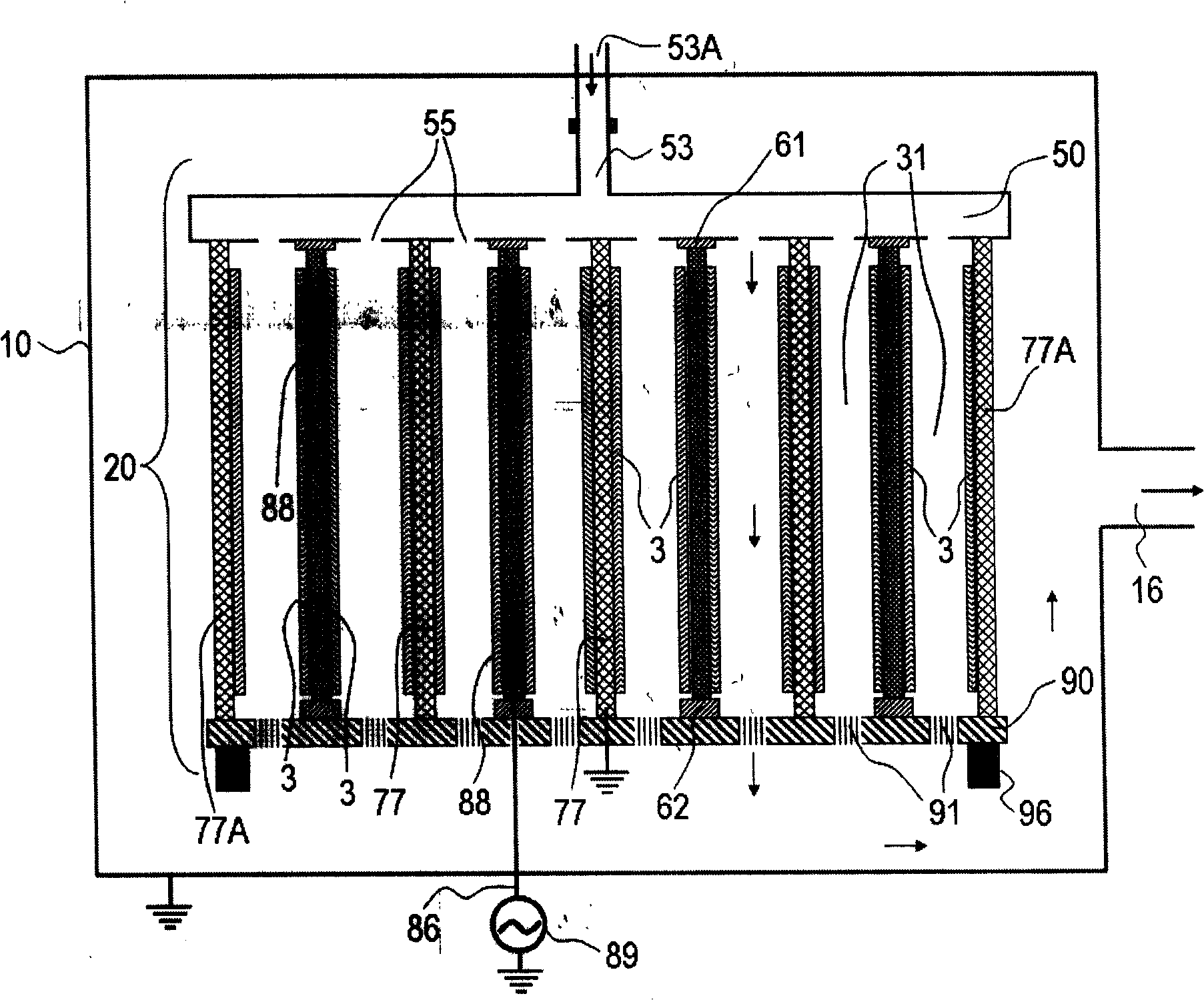
[0037] The invention relates to a method for manufacturing thin-film silicon p-i-n photovoltaic devices with high output and low cost by using a movable plasma box with multiple electrodes. The movable plasma box runs through all the steps related to thin film silicon photovoltaic layer coating, and always moves with the substrate. The following production example is a best description of the present invention.

[0038] Figure 5 Is a flow chart, it shows a typical adoption such as image 3 The PECVD system shown is the procedure for producing large quantities of double junction p-i-n thin-film silicon photovoltaic devices.

[0039] In the first step S1, the new tin oxide-plated glass substrate 3 is loaded into the movable plasma box 20 placed on the transport vehicle.

[0040] In the second step S2, the plasma box 20 is transferred into Figure 4 The shown preheating chamber 9 is heated to a preset temperature in the range of 160-260°C.

[0041] In the third step S3, the heated m...


PUM


Abstract

The invention discloses a plasma enhanced chemical vapor deposition (PECVD) device and a method for producing a large-area thin-film silicon photovoltaic device, and adopts a movable plasma chamber that can carry a plurality of electrodes and a large number of base plates and a single vacuum chamber. The production method of p-i-n type photovoltaic device based on thin-film silicon comprises the steps as follows: the base plates are put into the plasma chamber and then the plasma chamber is heated in a preheater furnace and put into the single plasma chamber of a PECVD system. A silicon film is deposited on the base plates in the fixed plasma chamber, and then the plasma chamber is moved from a PECVD vacuum chamber to a cooling chamber. Finally the base plates are taken out of the plasma chamber. The plasma chamber can be cleaned before processing the next group of the base plates. The method adopted by the invention is a simple production method with high throughput for the production of the photovoltaic device with low cost and high efficiency.

Description

technical field [0001] The present invention relates to a method for the industrial production of large-scale photovoltaic devices. In particular, it relates to a method for manufacturing a large-area thin-film silicon photovoltaic template with greatly improved productivity and reduced cost. Background technique [0002] In recent years, the development of thin-film photovoltaic devices and large-area templates has received worldwide attention. Especially hydrogenated amorphous silicon (a-Si) and nanocrystalline silicon (nc-Si) show great potential to play a pivotal role in applications such as building-integrated photovoltaics. An important feature of thin-film silicon photoelectric conversion devices (commonly known as solar photovoltaic cells and templates) formed at a relatively low temperature below 260°C is the use of well-established industrial coating equipment and procedures, by depositing silicon semiconductors and The film layer is electrically contacted to ach...

Claims


Application Information

Patent Timeline
IPC IPC(8): C23C16/513C23C16/52H01L21/205H01L31/0216H01L31/0264
Inventor 李沅民马昕
Owner BEIJING XINGZHE MULTIMEDIA TECH
Why Eureka
Try Eureka