Packaging conductive structure and its forming method

A conductive structure and conductive layer technology, applied in the direction of circuits, electrical components, electrical solid devices, etc., can solve problems such as open circuit, difficult deposition, semiconductor chip failure, etc.

Active Publication Date: 2008-08-20
CHIPMOS TECH INC
View PDF0 Cites 2 Cited by
  • Summary
  • Abstract
  • Description
  • Claims
  • Application Information

AI Technical Summary

Problems solved by technology

[0006] However, in the process of forming the conductive layer 151, since the deposition of the conductive layer is unidirectional deposition, it is indeed difficult to form a conductive layer with a sufficient thickness on the sidewall of the dielectric layer 13, which may easily lead to the risk of disconnection.
like figure 1 As shown by the dotted line in , part of the conductive layer 151 near the sidewall of the dielectric layer 13 is relatively difficult to deposit. Once the process is not properly controlled, it is very likely to cause an open circuit and cause the semiconductor chip to fail.

Method used


Image

  • Packaging conductive structure and its forming method
  • Packaging conductive structure and its forming method
  • Packaging conductive structure and its forming method

Examples


Embodiment Construction

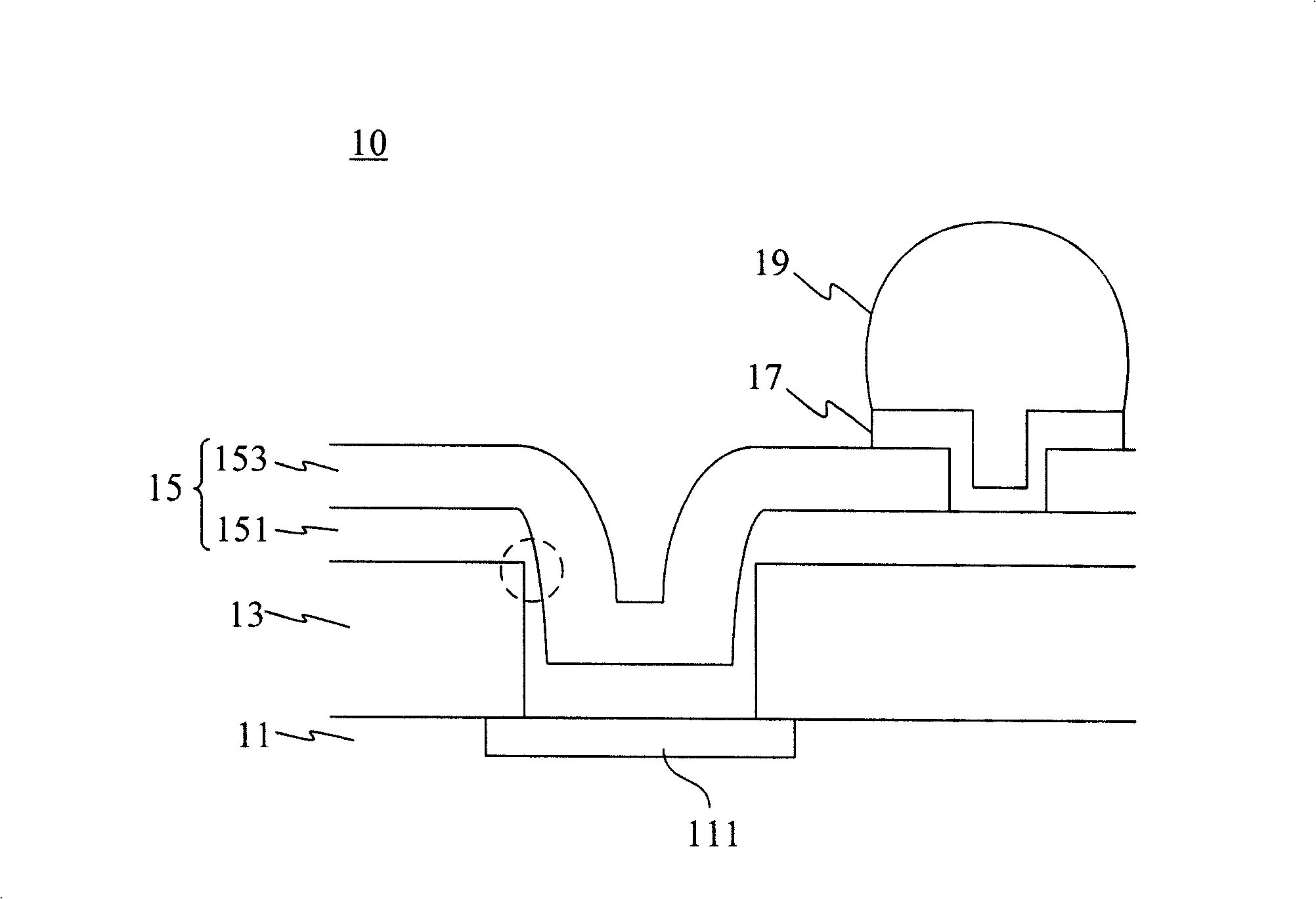
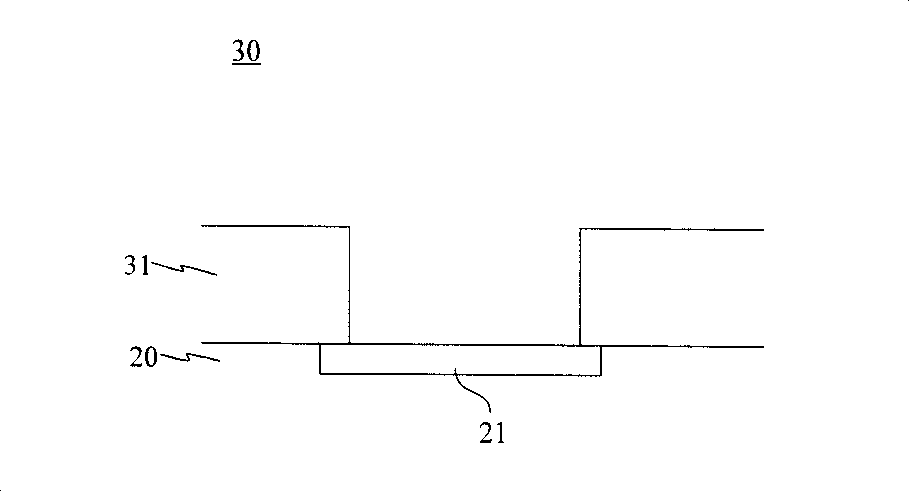
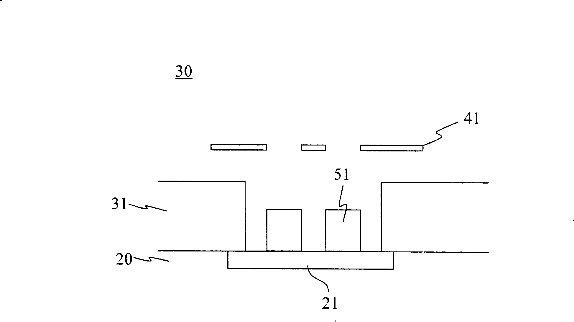
[0023] Please see first Figure 2A , the packaging conductive structure 30 of the present invention is applied to the semiconductor substrate 20, and the semiconductor substrate 20 usually has a metal layer 21, that is, a pad, as a contact for electrical connection. Generally speaking, the metal layer 21 is usually made of aluminum, and after being combined with the packaging conductive structure 30 of the present invention, subsequent electrical connection with other external components can be performed.

[0024] Firstly, a dielectric layer 31 is formed on the semiconductor substrate 20, which partially covers the metal layer 21 and defines an accommodating space so that the metal layer 21 can be partially exposed. More specifically, a large area of ​​dielectric material can be formed first, and then a photoresist layer (not shown) is partially formed on it, and then an etching process is performed to remove the part of the dielectric layer not covered by the photoresist laye...


PUM


Abstract

The invention relates to an encapsulated conducting structure for a semiconductor substrate and the forming method thereof. The dielectric layer of the encapsulated conducting structure is locally covered with the metal layer of the semiconductor substrate, and defines an accommodation space with an elevating layer and a conducting layer inside, the conducting layer stretches to connect with a bump, and the elevating layer is connected with a dielectric layer , so that the deposition of the edge of the dielectric layer is stabilized, and thus improving the reliability of the encapsulated conducting structure.

Description

technical field [0001] The present invention relates to an encapsulation conductive structure for a semiconductor substrate; in particular, an encapsulation conductive structure with a redistribution layer. Background technique [0002] Today's electronic products usually have semiconductor chips to provide control or logic operation functions. Due to the continuous improvement of process technology, semiconductor chips are becoming smaller and smaller, and the package size is gradually shrinking. [0003] The traditional wire bonding (Wire Bonding) method of bonding semiconductor chips and other components of the electronic packaging technology has long been insufficient, and it has been replaced by the flip-chip bonding technology that uses bumps as chips and other components. In other words, a plurality of bumps are provided on the surface of the semiconductor chip, which are electrically connected to the internal structure and are used for bonding with other components, ...

Claims


Application Information

Patent Timeline
Patent Type & Authority Applications(China)
IPC IPC(8): H01L23/485H01L21/60
CPCH01L24/11H01L2224/11H01L2924/14H01L2924/00H01L2924/00012
Inventor 黄成棠
Owner CHIPMOS TECH INC
Why Eureka
Try Eureka