Semiconductor device, semiconductor chip, method for testing wiring between chips and method for switching wiring between chips

A semiconductor and chip-to-chip technology, applied in the fields of semiconductor devices, semiconductor/solid-state device manufacturing, and electric solid-state devices, and can solve problems such as practical limitations

Inactive Publication Date: 2008-08-20
NEC CORP
View PDF2 Cites 17 Cited by
  • Summary
  • Abstract
  • Description
  • Claims
  • Application Information

AI Technical Summary

Problems solved by technology

Even when buried, e-fuses can be programmed, but such fuses are only just beginning to be used practically, so their usefulness is limited

Method used


Image

  • Semiconductor device, semiconductor chip, method for testing wiring between chips and method for switching wiring between chips
  • Semiconductor device, semiconductor chip, method for testing wiring between chips and method for switching wiring between chips
  • Semiconductor device, semiconductor chip, method for testing wiring between chips and method for switching wiring between chips

Examples


example 1

[0083] Next, the structure of the stacked semiconductor device of this working example will be described with reference to the drawings. FIG. 9 is a schematic view of a stacked semiconductor device of the present Working Example 1. FIG.

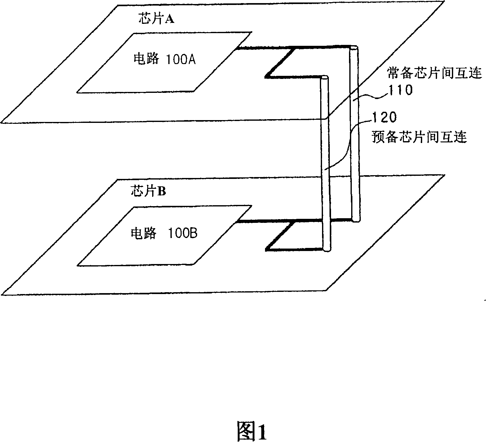
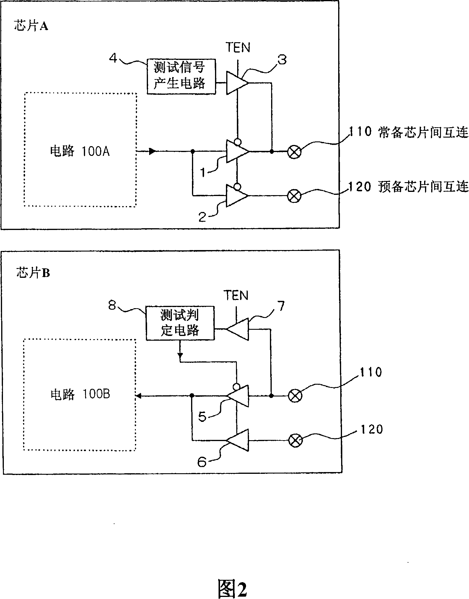
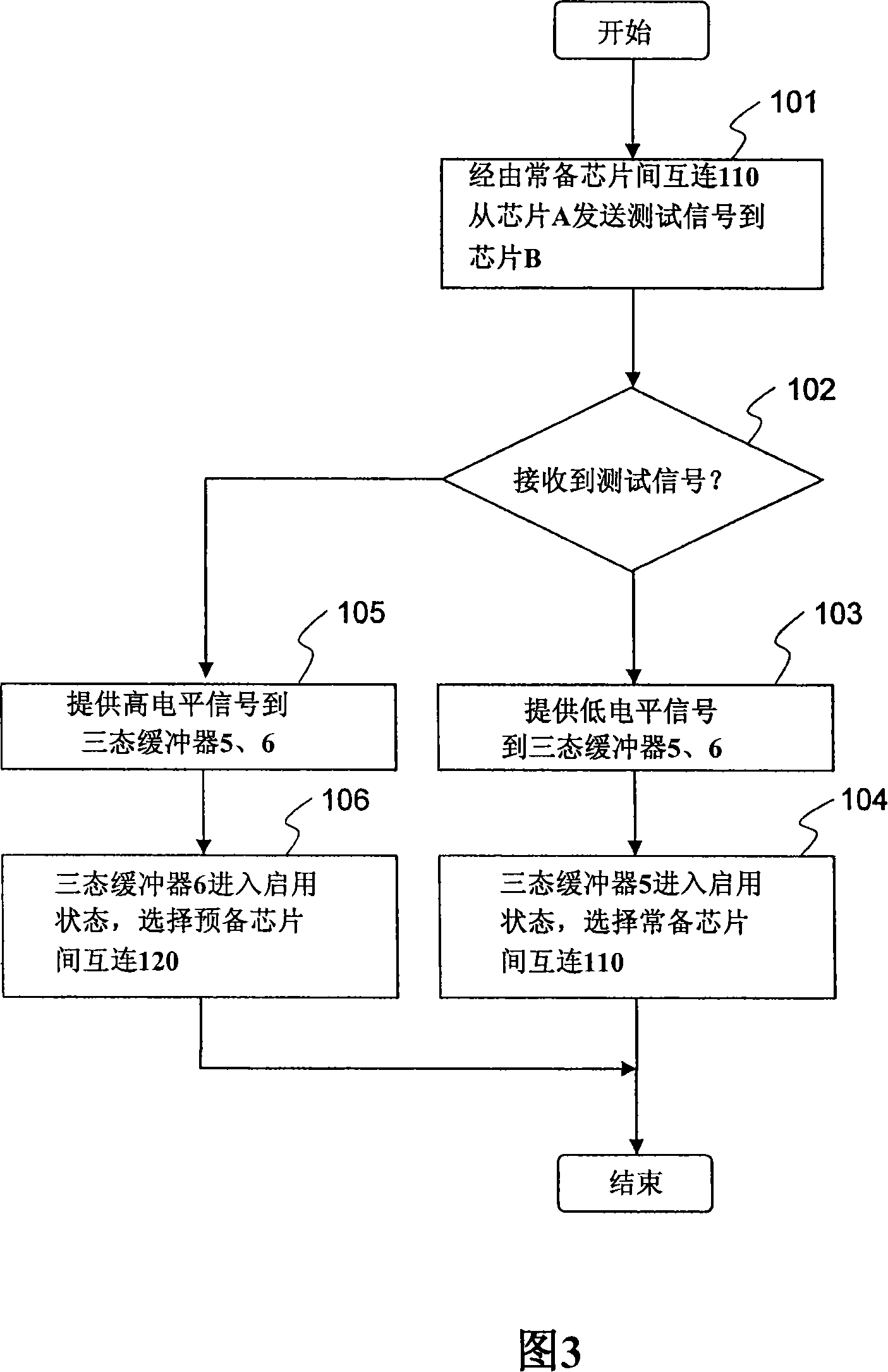
[0084] As shown in FIG. 9 , the stacked semiconductor device of this working example has a structure in which a chip A is stacked on a chip B. As shown in FIG. On chip A, a circuit 100A and a circuit 100A' are provided. On chip B, a circuit 100B and a circuit 100B' are provided. The connection between chips is realized through the regular inter-chip interconnect 111A, the regular inter-chip interconnect 111A′, and the spare inter-chip interconnect 121 .

[0085] In this working example, chip A and chip B are stacked, and in order to transfer signals from chip A to chip B, two regular interchip interconnects and one spare interchip interconnect are provided. When an electrical defect such as an open or short circuit occurs in any one of the...

example 2

[0106] The stacked semiconductor device of this working example is a device in which five chips are stacked.

[0107] FIG. 12A is a schematic view showing the structure of the stacked semiconductor device of this working example. FIG. 12B is a partially enlarged view of a redundancy switching portion shown by a dotted line in FIG. 12A.

[0108] As shown in FIG. 12A , the stacked semiconductor device has a structure in which a chip E, a chip D, a chip C, a chip B, and a chip A are sequentially stacked from the bottom. One spare interchip interconnect is provided for the four stock interchip interconnects between each chip. In FIG. 12A , the reference numerals of the regular interchip interconnect 112 and the preliminary interchip interconnect 122 are shown only for the interconnection between chip A and chip B. In FIG.

[0109] FIG. 12B shows the redundancy switching part of Chip C and Chip D. Here, to simplify the illustration, only one of the four stock interchip interconn...


PUM


Abstract

A semiconductor device is provided with a first wiring (110) between chips, for electrically connecting a first semiconductor chip with a second semiconductor chip; an auxiliary second wiring (120) between chips; a test signal generating circuit (4) for transmitting a test signal from the first semiconductor chip to the second semiconductor chip through the first wiring; a judging circuit (8), which outputs a first control signal in the case of receiving the test signal through the first wiring, and outputs a second control signal, i.e., the inversion signal of the first control signal, in the case of not receiving the test signal; and switching circuits (5, 6), which set the first wiring as a channel when the first control signal is inputted from the judging circuit, and set the second wiring when the second control signal is inputted.

Description

technical field [0001] The invention relates to a semiconductor chip, a semiconductor device with a plurality of semiconductor chips, an inter-chip interconnection testing method and an inter-chip interconnection switching method. Background technique [0002] With the miniaturization of semiconductor integrated circuits, the degree of integration has been increasing, progress has been made in increasing CPU performance and increasing memory capacity. However, there is a limit to the miniaturization of semiconductors, and new technologies to achieve greater integration are now required. As an example of such technology, a three-dimensional semiconductor in which semiconductor chips are stacked is proposed. [0003] A method for laminating semiconductor chips to realize a large-scale integrated circuit without changing the chip area disclosed in JP-A-H04-196263 (hereinafter referred to as Patent Document 1), in which a memory circuit is integrated in a semiconductor integrat...

Claims


Application Information

Patent Timeline
Patent Type & Authority Applications(China)
IPC IPC(8): G01R31/28H01L21/822H01L27/04
CPCG01R31/2812G01R31/2853G01R31/31717
Inventor 斋藤英彰
Owner NEC CORP
Why Eureka
Try Eureka