Inspection method and apparatus, lithographic apparatus, lithographic processing cell and device manufacturing method

A technology for inspection equipment and lithography equipment, which is used in electrical components, optomechanical equipment, microlithography exposure equipment, etc.

Inactive Publication Date: 2008-08-27
ASML NETHERLANDS BV
View PDF2 Cites 15 Cited by
  • Summary
  • Abstract
  • Description
  • Claims
  • Application Information

AI Technical Summary

Problems solved by technology

[0019] 2. The phase modulator is wavelength dependent, which means that the phase modulator must be recalibrated for each wavelength used

Method used


Image

  • Inspection method and apparatus, lithographic apparatus, lithographic processing cell and device manufacturing method
  • Inspection method and apparatus, lithographic apparatus, lithographic processing cell and device manufacturing method
  • Inspection method and apparatus, lithographic apparatus, lithographic processing cell and device manufacturing method

Examples


Embodiment Construction

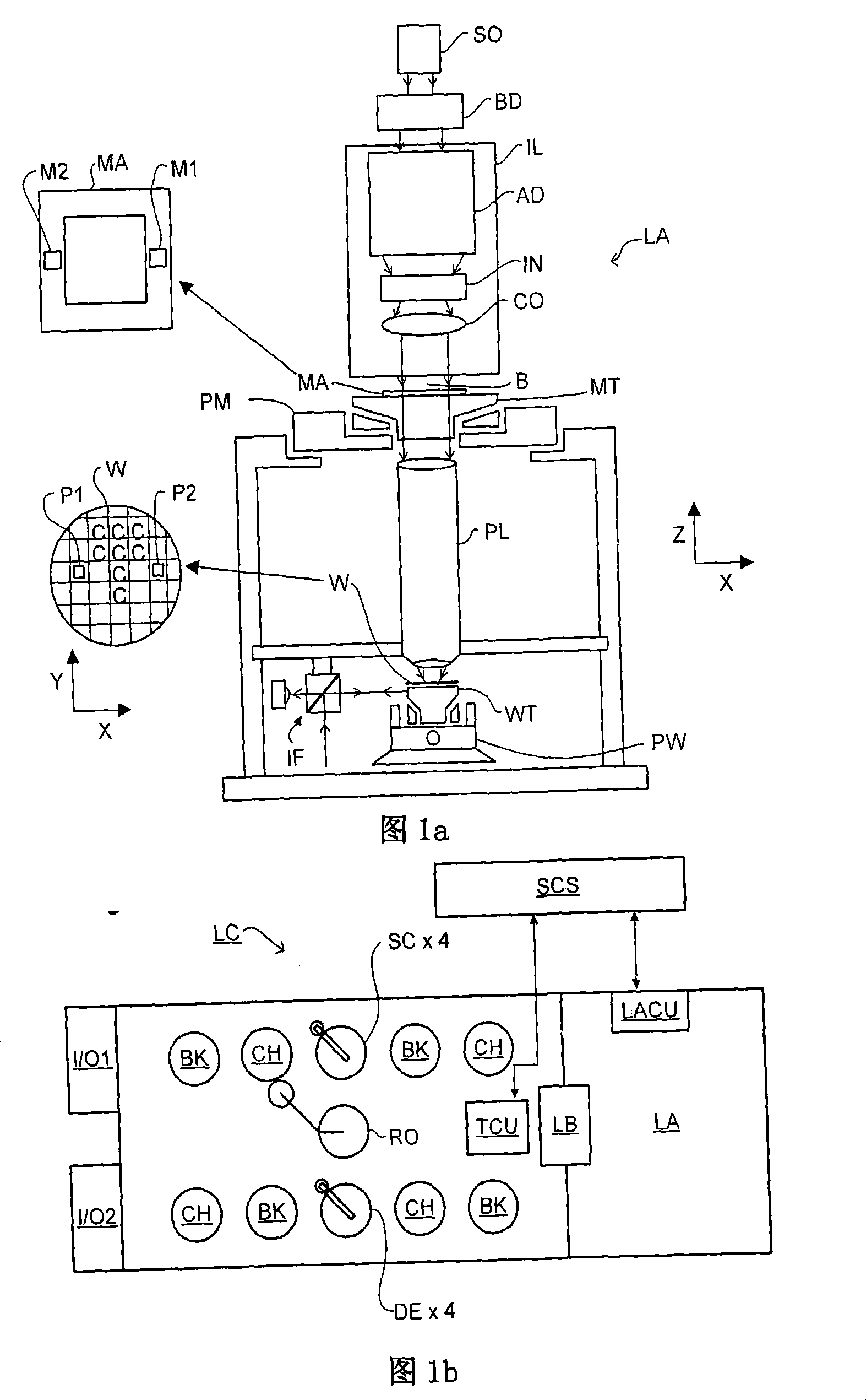
[0044] Figure 1a schematically shows a lithographic apparatus. The apparatus comprises: an illumination system (illuminator) IL configured to condition a radiation beam B (e.g., ultraviolet radiation or deep ultraviolet radiation); a support structure (e.g., a mask table) MT configured to support a patterning device (e.g., mask) MA and is connected to a first positioner PM configured to precisely position the patterning device according to determined parameters; a substrate table (e.g. wafer table) WT configured to hold a substrate (e.g. coated with a resist agent wafer) W connected to a second positioner PW configured to precisely position the substrate according to determined parameters; and a projection system (such as a refractive projection lens system) PL configured to The pattern imparted by the patterning device MA to the radiation beam B is projected onto a target portion C of the substrate W (eg, comprising one or more dies).

[0045] The illumination system may inc...


PUM


Abstract

The present invention discloses a inspection method and apparatus, photolithography apparatus, photolithography unit and device manufacturing method. Particularly the present invention refers to the simultaneous measurement of four separately polarized beams upon diffraction from a substrate in order to determine properties of the substrate. Circularly or elliptically polarized light sources are passed via up to three polarizing elements. This polarizes the light sources by 0, 45, 90 and 135 DEG . The plurality of polarizing beam splitters replaces the use of a phase modulator, but enables the measurement of the intensity of all four beams and thus the measurement of the phase modulation and amplitude of the combined beams to give the features of the substrate.

Description

technical field [0001] The present invention relates to an inspection method that can be used, for example, in the manufacture of devices by photolithography, and to a method of manufacture of devices using photolithography. Background technique [0002] A lithographic apparatus is a machine that applies a desired pattern onto a substrate, usually onto a target portion of the substrate. For example, lithographic equipment may be used in the manufacture of integrated circuits (ICs). In this case, a patterning device, alternatively referred to as a mask or reticle, may be used to generate the circuit pattern to be formed on the individual layers of the IC. The pattern can be transferred onto a target portion (eg, a portion including a portion of a die, one or more dies) on a substrate (eg, a silicon wafer). Typically, the pattern is transferred via imaging to a layer of radiation sensitive material (resist) provided on the substrate. Typically, a single substrate will conta...

Claims


Application Information

Patent Timeline
Patent Type & Authority Applications(China)
IPC IPC(8): G03F7/20G01J9/00G01B11/24
CPCG01B11/0641G01N2021/4711G01N2021/4792G03F7/70625G03F7/70633H01L22/00
Inventor 亚历山大·斯卓艾杰尔罗纳德·弗朗西斯科斯·赫尔曼·休格斯
Owner ASML NETHERLANDS BV
Why Eureka
Try Eureka