Wafer-level burn-in method and wafer-level burn-in apparatus

An aging device, wafer-level technology, applied in measurement devices, instruments, measurement electronics, etc., can solve problems such as difficulty in ensuring wafer temperature

Inactive Publication Date: 2008-08-27
PANASONIC CORP
View PDF0 Cites 13 Cited by
  • Summary
  • Abstract
  • Description
  • Claims
  • Application Information

AI Technical Summary

Problems solved by technology

[0013] From the above, it is difficult to keep the temperature of the wafer at around 125°C with the structure shown in Figure 4

Method used


Image

  • Wafer-level burn-in method and wafer-level burn-in apparatus
  • Wafer-level burn-in method and wafer-level burn-in apparatus
  • Wafer-level burn-in method and wafer-level burn-in apparatus

Examples


Embodiment Construction

[0038] Hereinafter, embodiments of the present invention will be described with reference to the accompanying drawings.

[0039] (Embodiment 1)

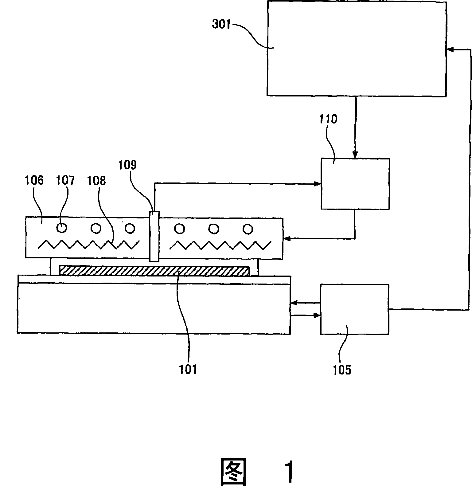
[0040] FIG. 1 is a schematic diagram of a wafer-level burn-in apparatus in Embodiment 1 of the present invention. The first embodiment shown in FIG. 1 is a configuration obtained by adding a temperature correction value calculating device 301 to the device configuration shown in FIG. 4 .

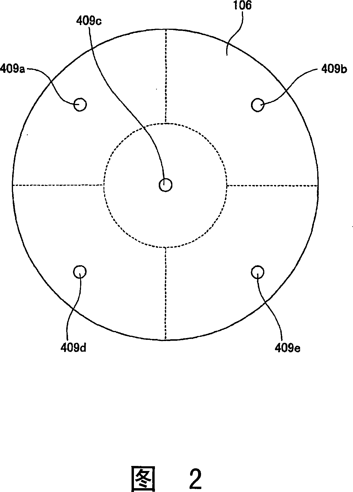
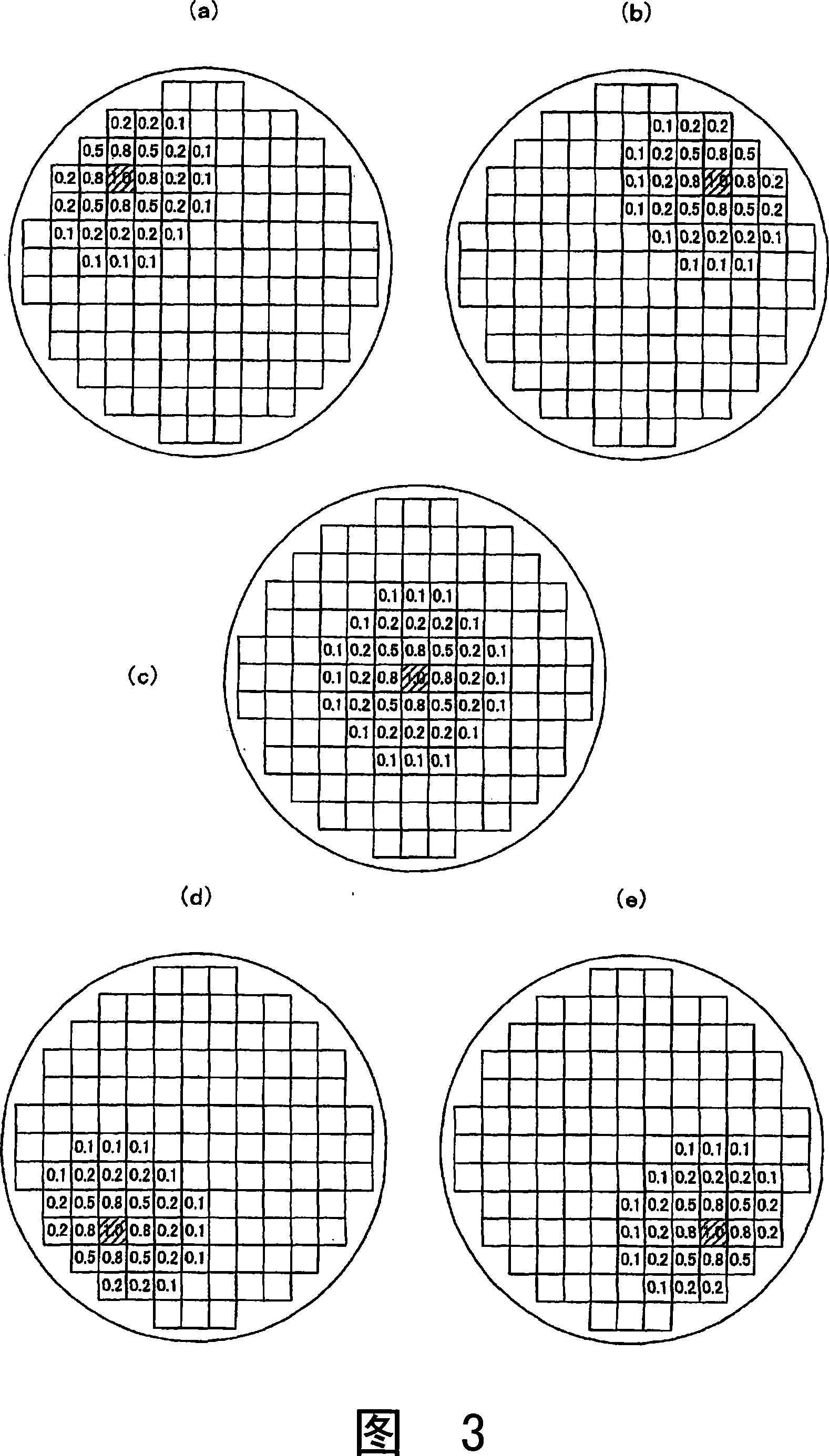
[0041] In the wafer-level burn-in according to the first embodiment using such a structure, experiments are performed in advance to test the wafer 101 caused by heat generated by power consumption on the device when an electrical load is applied to the device formed on the wafer 101. The difference between the actual temperature of 101 and the temperature measured by the temperature sensor 109 is calculated as a function of the amount of heat generated per unit area on the wafer 101 , that is, the heat generation density. In this Embodiment 1, th...


PUM


Abstract

The invention provides a wafer-level burn-in method and a wafer-level burn-in apparatus. A temperature control in a wafer-level burn-in test is performed in such a way that a set temperature used for the temperature control is corrected using a correction value calculated from the generated heat density of a wafer (101). This eliminates the difference between the temperature of the wafer heated when an electrical load is applied and the control temperature for applying a thermal load, not depending on the distribution of good devices formed on the wafer (101) and the device's power consumptions. As a result, the wear and burn of probes can be prevented and a highly reliable screening can be performed.

Description

technical field [0001] The present invention relates to a wafer-level aging method and a wafer-level aging device for applying electrical load and temperature load to a semiconductor wafer for screening. Background technique [0002] In the past, a screening test device, generally called a burn-in device, encapsulates an IC chip obtained by dicing a semiconductor wafer, and then conducts an energization test in a hot atmosphere at a predetermined temperature (for example, 125°C) to make latent defects obvious. Screening of non-conforming products. [0003] Since such a conventional device requires a large thermostat and generates a large amount of heat, it must be separated from other production lines and performed in other rooms, and it takes time and effort to transfer wafers, install into the device, and assemble and disassemble. In addition, because unqualified products are found after packaging, the packaging cost will be wasted, and because there is a requirement that...

Claims


Application Information

Patent Timeline
Patent Type & Authority Applications(China)
IPC IPC(8): H01L21/66G01R31/26
CPCG01R31/2874H01L21/67248G01R31/26H01L22/00
Inventor 濑川彰继真田稔
Owner PANASONIC CORP
Why Eureka
Try Eureka